This is the fourth in my series of Z80 retrocomputing blog posts.
For background, I suggest starting with the first post.
So what exactly is the purpose of the bus supervisor board? I wanted to do some assembly language work on the RC2014 Z80 Retrocomputer, and I examined several options:
- I could program an EPROM with my assembly language program, run it, then when it was time for the revision I could pop the EPROM out, erase and reprogram it, and repeat the cycle. I’ve done this before, and it’s a slow development cycle. You’re spending lots of time erasing and reprogramming EPROMs.
- I could write a bootloader and store that in the EPROM, and the bootloader could load a program from the serial port, or from an attached SD card, write that program to RAM, and execute it. This improves upon approach #1 by eliminating the need to erase and reprogram EPROMs. It requires some effort to local and/or write a boot loader.
- I could ditch the EPROM altogether, put some static RAM in its place, and come up with a way to program the static ram in-circuit.
The bus supervisor implements approach #3. I’m going to get rid of the RC2014’s ROM board, install a dual-RAM board in it’s place. Then I’m going to attach a raspberry pi to the Z80’s bus, let it put the Z80 to sleep, and have the pi program the RAM chip.
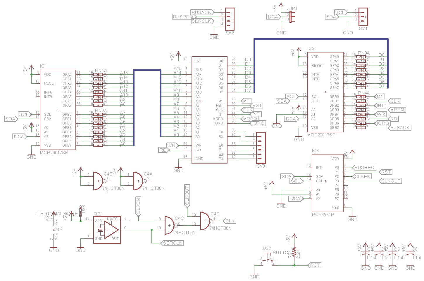
In order to seize control of the Z80’s bus, I’m going to use some io expander chips attached to the pi, and connect each of the Z80’s address, data, and control pins to the io expander. This will let the pi read and write those pins. Let’s see the schematic:
Taking a look at the above schematic, we can see three IO expanders. Two are MCP23017 and one is a PCF8574. The MCP23017 are 16-bit IO expanders, and are by far the more versatile of the two chips, featuring configurable pull-ups, many different interrupt modes, etc. The PCF8574 is a much simpler chip and features only 8 bits of IO. We only need about 36 bits of IO to make this project work, so I opted to go with two MCP23017 and one PCF8574.
The MCP23017 and PCF8574 are both I2C devices, and they can communicate with the raspberry pi over a 3-pin (SDA, SCL, GND) i2c bus. I’ve used I2c in several of my projects. It’s really convenient and makes it easy to add peripherals to the pi.
As you can see, the entire address (A0..A15), data (D0..D7), and the majority of the control (M1, IORQ, MREQ, RD, WR, RESET, CLK, INT, BUSREQ, BUSAK) are connected to the IO expanders. They’re connected via some dip resistor packs. These aren’t necessary for correctness; they’re install to have some protection against operator error. If I program the MCP23017 incorrectly, then it would be possible to be outputting a “1″ on some pin while the Z80 is outputting a “0″, allowing current to flow in an undesirable way (perhaps burning out an IO line on one device or the other). The resistors limit the amount of current that can flow in the event of a mistake. I chose to use 470 ohm resistors, on the basis that it’s what I had in the junk box.
Also on the board is a clock generator. The supervisor board replaces the RC2014’s default clock board. The reason for this is twofold: 1) save on backplane space, and 2) to be able to stop the clock or implement a slow clock. I use a 7.3728 Mhz crystal oscillator, and it’s connected to a pair of NAND gates. If the CLKEN (PCF8574 output #3) signal is low then the on-board oscillator will be disabled. Outputting a squarewave on the CLKOUT (PCF8574 output #4) signal can then clock the Z80.
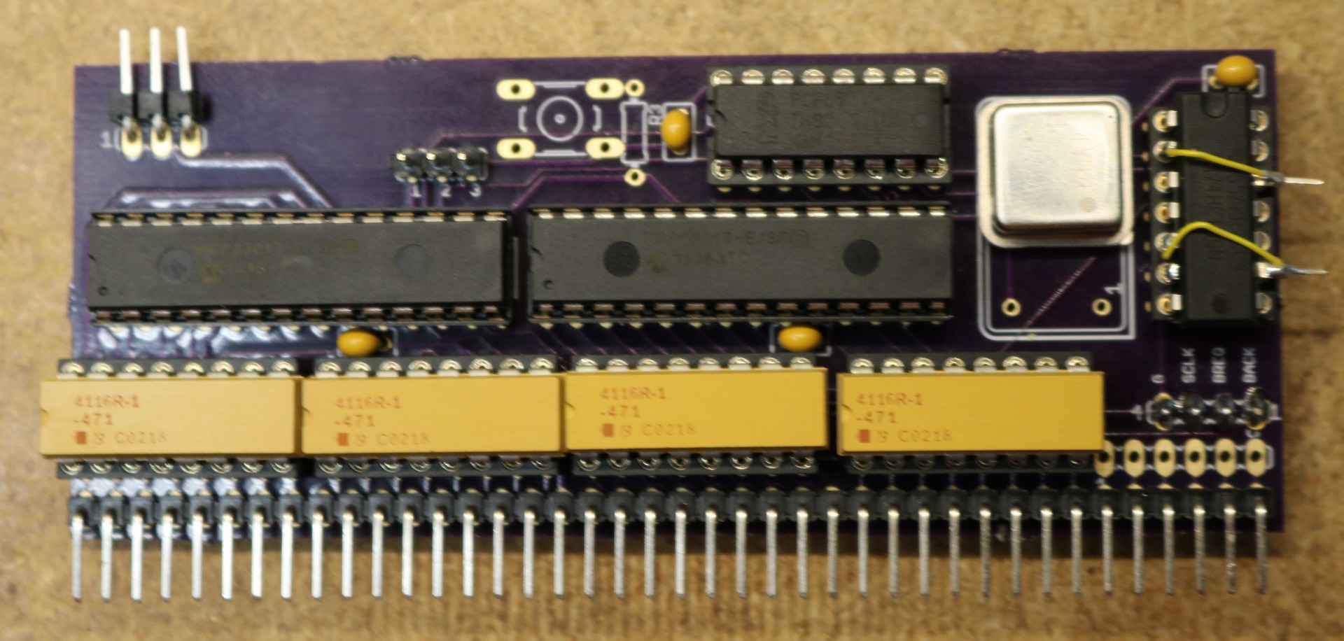
Here’s a picture of the completed Bus Supervisor board:
It may be obvious (particularly from the little yellow wires) that there’s a few mistakes in the above board. These have already been corrected in the schematic. The next time I fab the pcboard (if there is a next time), I’ll correct the imperfections.
Seizing control of the Z80 bus
Okay now to the software… Our first task is to seize control of the Z80 bus. It’s handy that the Z80 provides a pair of pins for just this purpose. If we make BUSREQ low, then the Z80 will give up the bus, and everything important goes into tristate. Once it’s done this, it’ll set BUSACK low. Once we see BUSACK is low, the bus is ours to do with as we please. We need to reconfigure our MCP23017 io expanders so that the relevant pins are outputs instead of inputs. Then the pi can write to those IO pins. For example, we can put an address on the address bus, set RD and MREQ low, and then read the data bus. That’s how we can examine a memory address.
In a similar manner, we can also write memory (set WR low instead of RD), and we can read and write IO ports (set IORQ low instead of MREQ). This allows the raspberry pi to interact with the Z80’s memory and IO devices.
We can dump a RAM chip by looping through all of the addresses, issuing a read of each one, and then writing the result to a file. We can do the reverse by reading a file, looping through all of the addresses, and issuing a memory write for each one.
When we’re done, we simply set BUSREQ back to high, and the Z80 will resume whatever it was doing.
Resetting the Z80
Since the PCF8574 io expander is connected to the reset pin, all we need to do to is set RESET low and then return it to high again.
Source Code
The source code for the supervisor program is available in my github repo at http://www.github.com/sbelectroncs/rc2014.

