Quantcast
Channel: Electronics Projects – Dr. Scott M. Baker
Viewing all 118 articles
Browse latest View live

Polaroid 312 LED Camera Light – Teardown and Repair

$
0
0

My camera light has been having issues almost since I bought it, so I tore it apart:

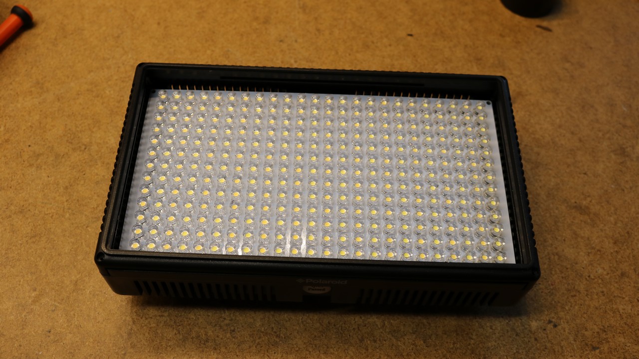
Here’s a picture of the light, it’s made by Polaroid. I bought it at Amazon.

Polaroid 312 LED Camera Light

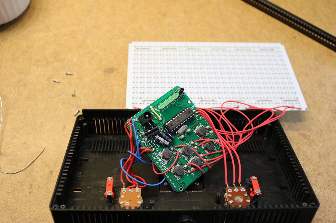
Unfortunately, I didn’t take many still shots while I was disassembling it (see the youtube video at the top for the teardown video). The only still I took was this one:

Polaroid 312 LED Camera Light, disassembled

The problem I was experiencing was that the light would occasionally turn off on it’s own, and I’d have to turn it back on. The problem turned out to be a poor solder joing on the crystal next to the microcontroller. The solder had balled up on the crystal’s lead, rather than adhering to the PCB pad. As such, I think as the light heated up, thermal expansion would cause the lead to lose contact with the pad, and glitch the microcontroller. Shutting the light off and turning it back on would ‘reboot’ the microcontroller.

Also interesting in this teardown is that they appeared to use masking tape (yes, like from Home Depot’s paint department) as a shield between the PCB and the LED array. Stuck to this masking tape was  what appeared to be a cut off piece of through-hole resistor lead — it’s a wonder it didn’t short something out.


RGB Rotary Encoder on a Raspberry Pi

$
0
0

I interface an RGB Rotary Encoder to my Raspberry Pi:

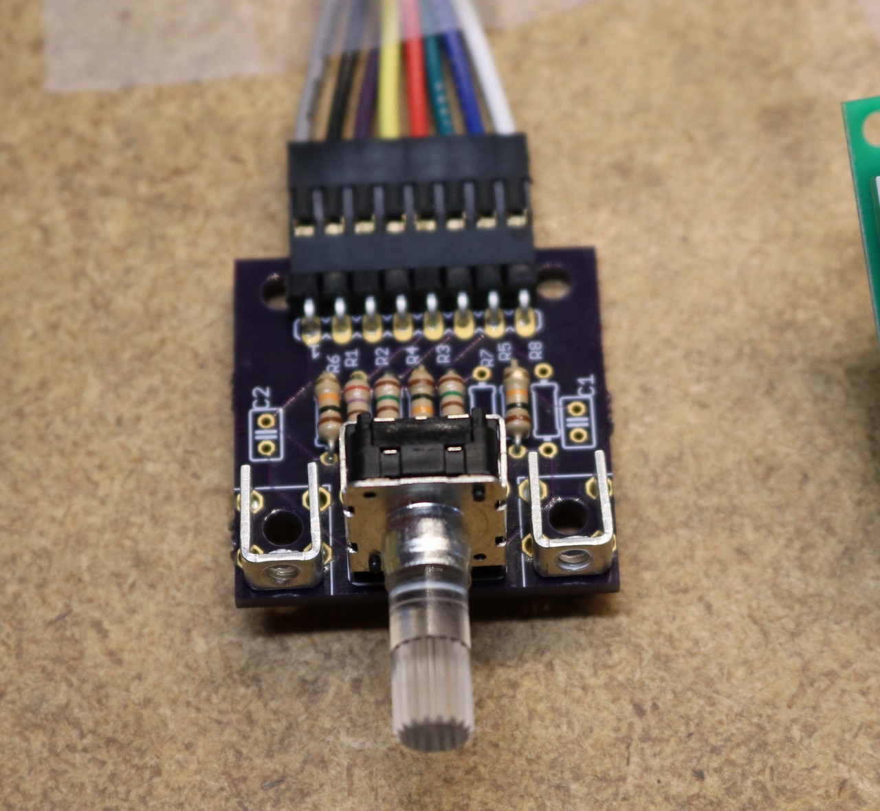
I really should have taken some more pictures…  I suggest watching the video for most of the details — I actually whiteboarded the schematic and went through it. I did manage to design a breakout board, and it’s pictured below:

RGB Rotary Encoder Breakout Board

The Rotary Encoder is from SparkFun, com-10984. That’s the right-angle version. There’s also a vertical version, COM-10982, with a slightly different footprint.

The Rotary encoder has a total of 8 pins. Three of them are for the encoder itself:

  • Common
  • A
  • B

The other 5 are for the LED and the switch:

  • Red
  • Switch
  • Green
  • Blue
  • V+

There’s some code on the encoder demo checked into github at https://github.com/sbelectronics/pi-encoder. The thing was fairly easy to interface, and I made use of a library that Guy Carpenter had written as part of py-gaugette. Unfortunately, it’s not a gray-code encoder, but is a standard incremental quadrature encoder. You watch the A and B lines and depending on how they transition, you’re able to determine the direction and the number of steps that have turned. How the encoder works is explained in my video at the top of the page.

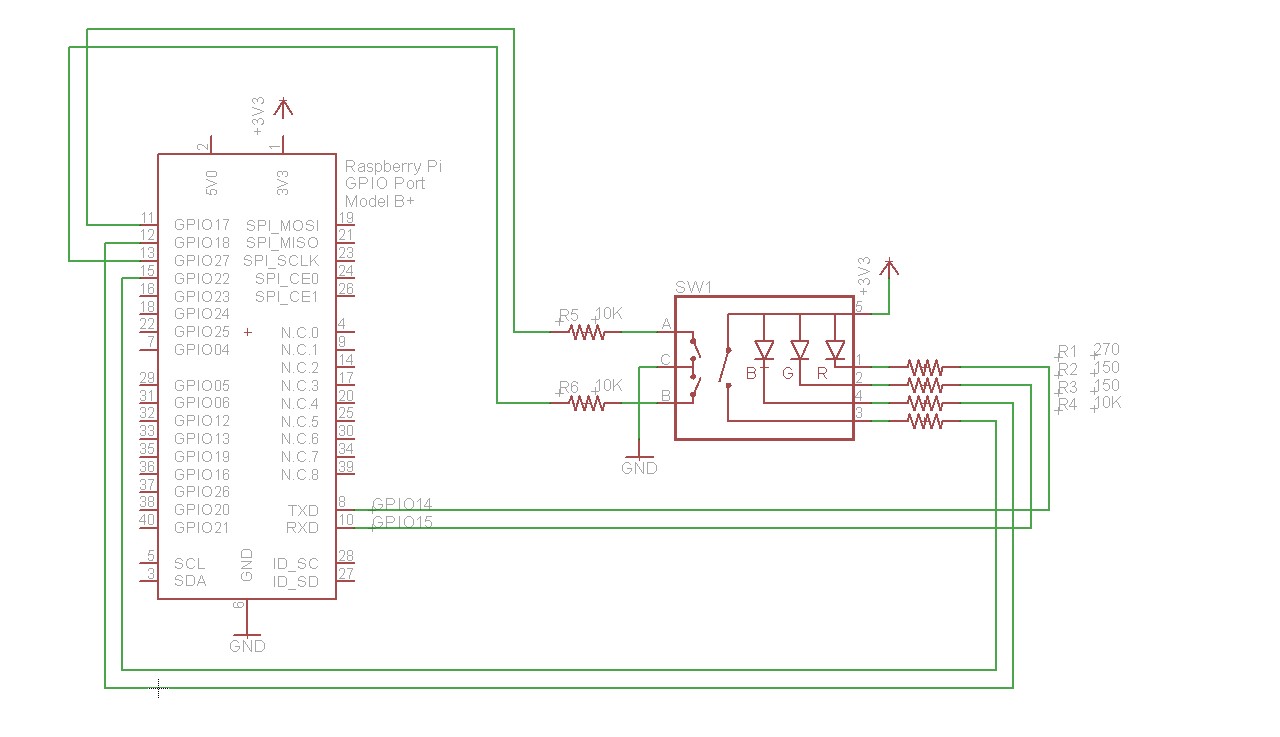
The LED has three elements for red, green, and blue respectively, and you can PWM them to get various shades of colors. The switch is a simple pushbutton — push in on the encoder shaft. This schematic shows which GPIO pins I connected it to on the pi:

Raspberry Pi RGB Encoder Schematic

Raspberry Pi RGB Encoder Schematic

I went on to use this encoder in my digital attenuator project.

Sinometer VC2000 Frequency Counter Review

$
0
0

A while ago, I purchased a frequency counter for my RF projects:

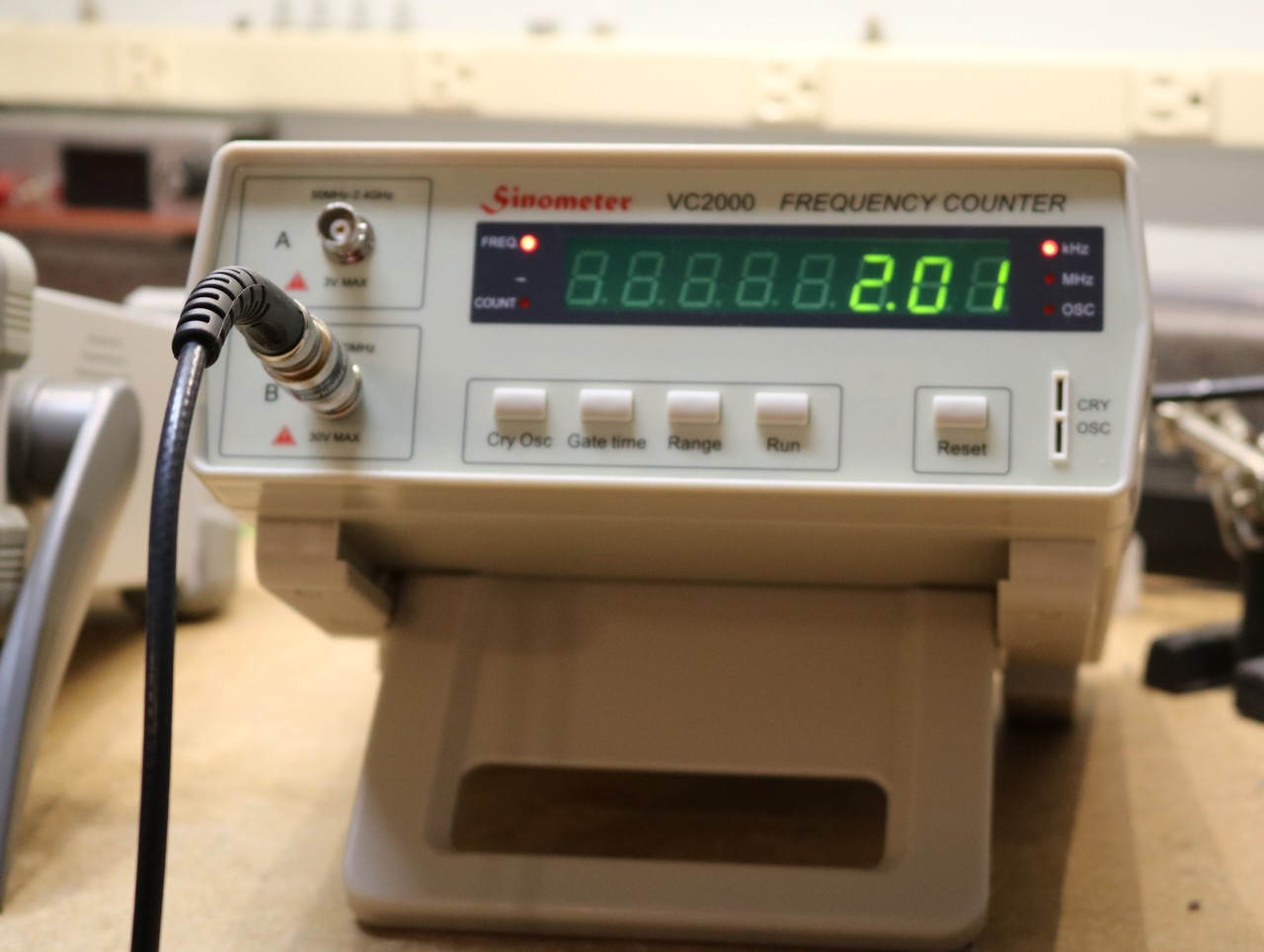
This particular frequency counter has a range from 10Hz to 2.4GHz. I’ve only tested it up to a few hundred megahertz because that’s all the higher my various frequency generators go. You can buy this counter for under a hundred bucks on Amazon, it seems like a pretty good deal. Here’s a high-resolution shot of the generator:

Sinometer VC2000 Freqeuncy Generator

Sinometer VC2000 Frequency Generator

I’ve used this in several projects — reading out the marker frequency in my sweep generator, setting up my DIY RF generator to verify the ebay counter was working properly, etc. A standalone frequency counter is a handy tool to have, but it’s probably not essential. Many modern digital storage oscilloscopes will have built in counters, though I haven’t found the one in my Rigol DS1054Z to be quite as accurate. Even my Siglent arbitrary waveform generator has a built in frequency counter feature.

There’s a few user interface annoyances with the Sinometer VC2000. It has several different ranges which are identified numerically. The first range corresponds to the “A” BNC jack. The second and third ranges correspond to the “B” BNC jack. Another range is used for measuring period, and another for operating in count mode. You sort of have to keep these ranges memorized, or have the manual handy.

I was pleasantly surprised at the overall construction — the video at the top of this post will show a quick teardown. For < $100, it seems like a fairly decent instrument.

DIY Digital RF Attenuator

$
0
0

I build a digital RF attenuator for the bench:

So what do I need a digital RF attenuator for? This started out with my DIY RF Generator project. I started out trying to use a plain ordinary potentiometer as my RF output control, and found that it screwed the output impedance all up. Then I bought a stepped RF attenuator on eBay, and found that it was too large to fit inside my case. Then I figured, well I’ll just build my own stepped attenuator, and I’ll make it digitally controlled, and I started researching designs for this. My original plan was to use a bunch of pi-attenuator circuits switched by relays.

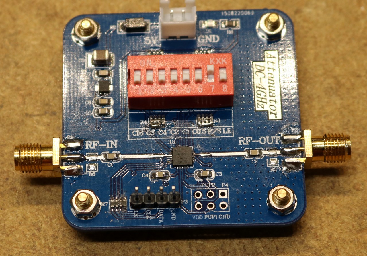
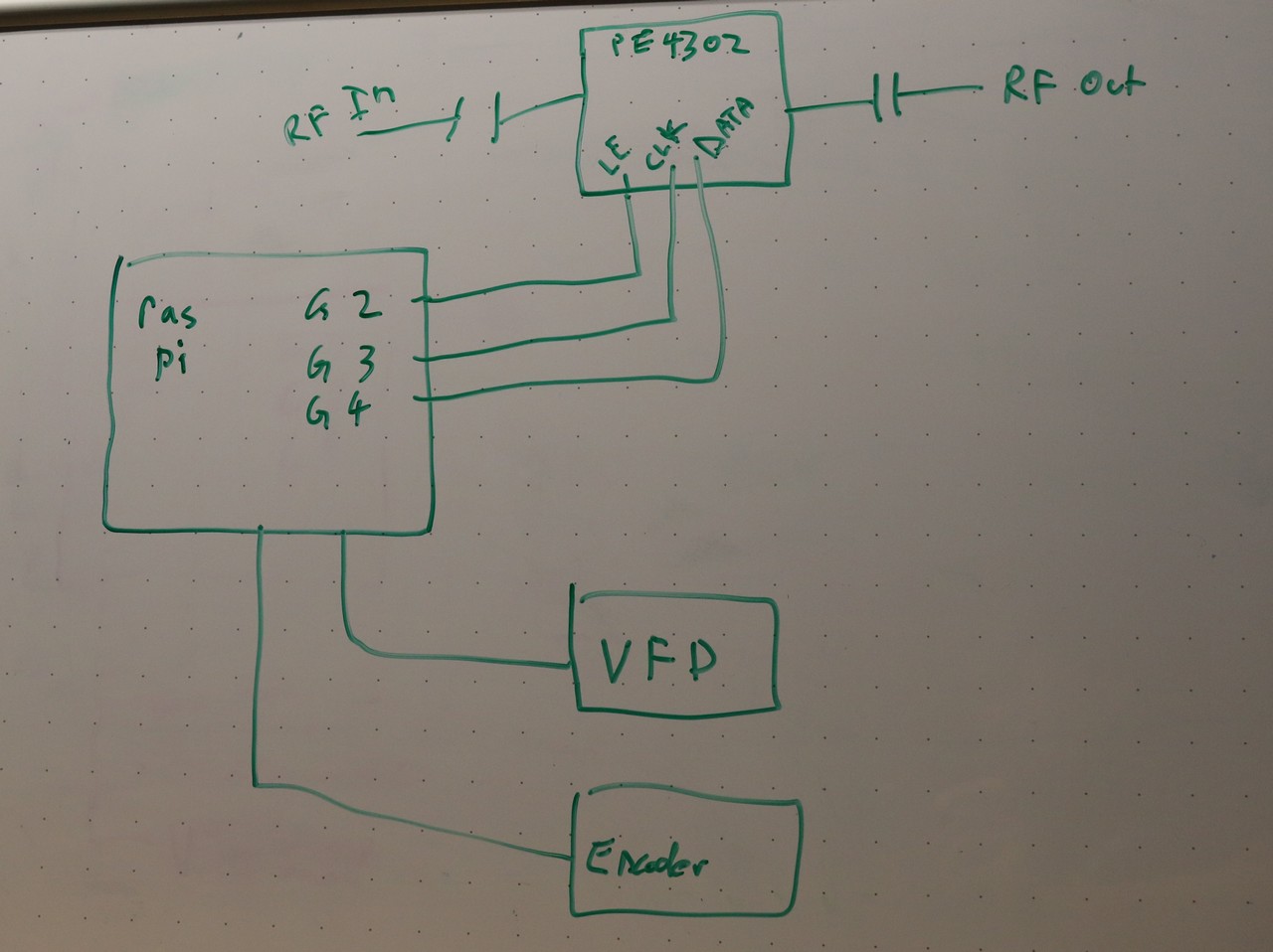
I found out that there’s an existing chip, the PE4302, that does this all electronically. It includes 6 steps, each an individual pi-attenuator circuit, and allows them to be switched into circuit. It has a simple serial protocol that can be used, basically just a clocked latch. I ordered a PE4302 breakout board from eBay:

PE4302 breakout board

PE4302 breakout board

The overall project is a combination of this breakout board, together with my RGB encoder project and my VFD project:

Digital stepped RF attenuator, whiteboard schematic

Digital stepped RF attenuator, whiteboard schematic

I haven’t drawn in the connections for the VFD and Encoder; you can check other blog posts for those. The PE4302 is connected to GPIOs 2, 3, and 4. The PE4302 works just like a shift register — you clock in 6 data bits, and then you toggle a latch line to load the shift register into the attenautors output. If gives you 64 steps in 0.5dB increments, from 0 to 31.5dB of attenuation.

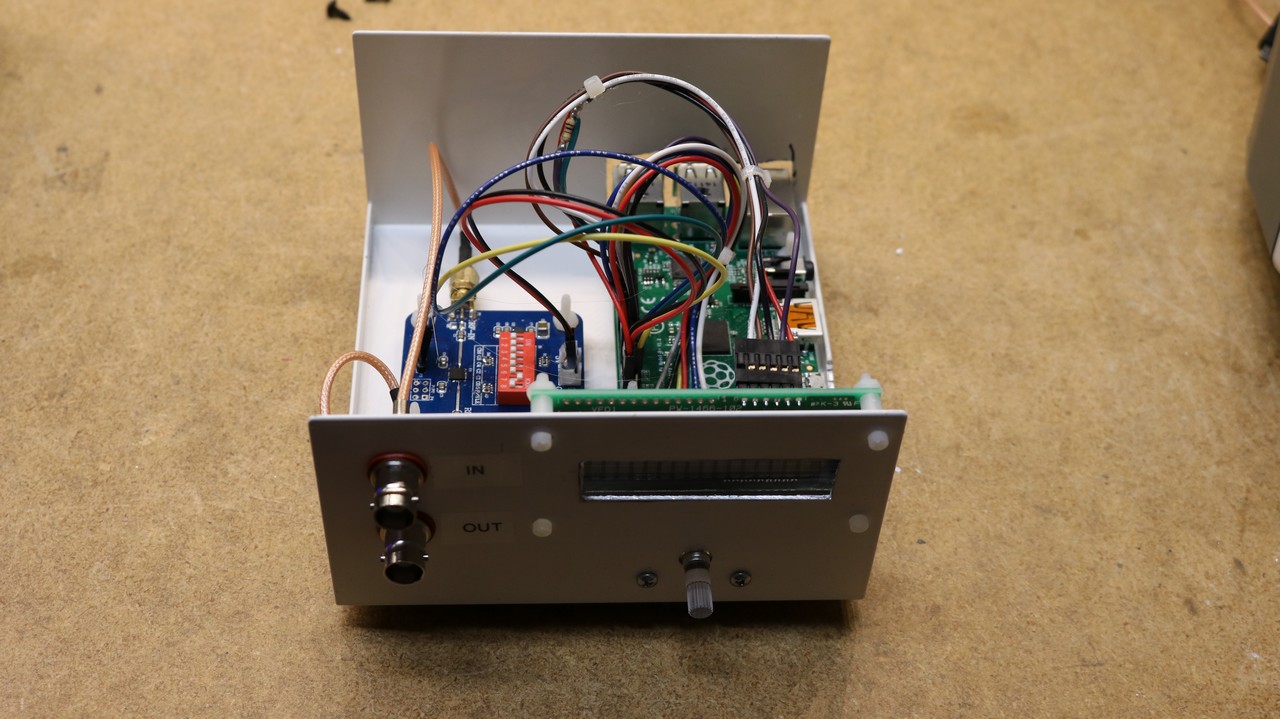
I assembled it all in a jameco instrument box and here is the result:

Digital RF attenautor, with the lid off

Digital RF attenuator, with the lid off

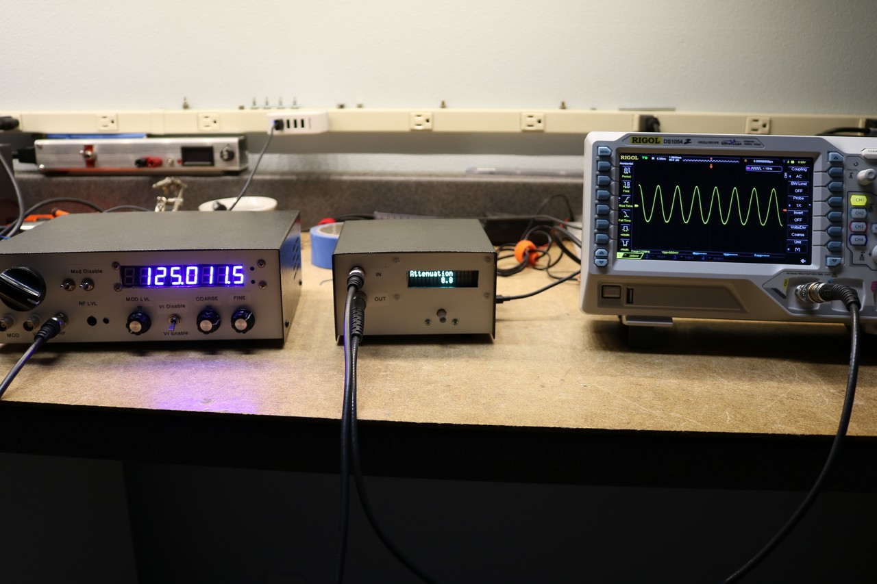
Here’s a view of the attenuator in action:

Digital stepped attenuator, in use

As you can see, I have it connected between my DIY RF generator and my rigol DS1054Z.

Eico 369 RF Sweep Generator

$
0
0

There’s something fun about using period tools to work on old radios:

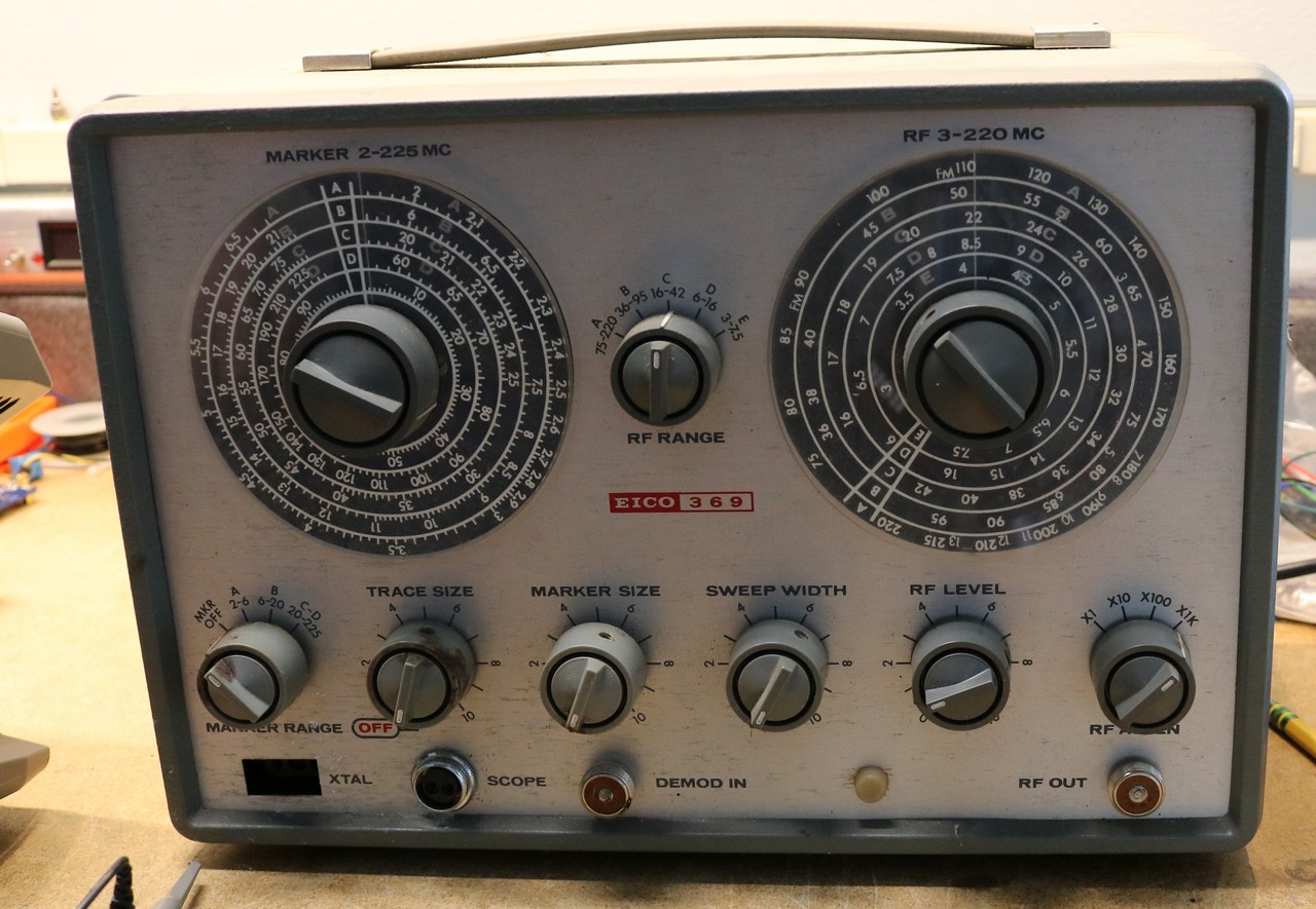
This is my second tube RF generator, and my fifth RF generator overall. Why did I buy this one? I think having an old-school RF sweep generator is both fun, and it’s the type of that the instructions that tell you how to align the old radios expect you to be using. Let’s start with some pictures of the Eico 369:

Eico 369 RF Generator, unmodified, as it arrived

Let’s take a small tour of the controls. The dial on the left is the marker osciallator frequency. The marker oscillator puts a blip on the output so you can see a specfic spot during the sweep. My video makes it obvious how this works, and I’ll try to describe it below in text as well. The dial on the right is the sweep oscillator center frequency. Between the two big dials is the range of the sweep oscillator. It’s usable from 3Mhz all the way up to 220Mhz.

Starting with the small dials, working left to right, the first is the marker range. It allows you to select the range of the marker oscillator, from 2Mhz up to 225Mhz. The next is the trace size, which controls how large the demodulated swept trace is on your scope. Next is marker size, which determines how big the marker blip is. Sweep width lets you control how wide the sweep is. The final two are an RF pot and an RF stepped attenuator.

You can see it has the weird microphone connector RF probe jacks that are typical of 50s and 60s RF test gear. One of the first things I did was replace those with BNC jacks.

Now for some inside pictures. Let’s start with a view from the top:

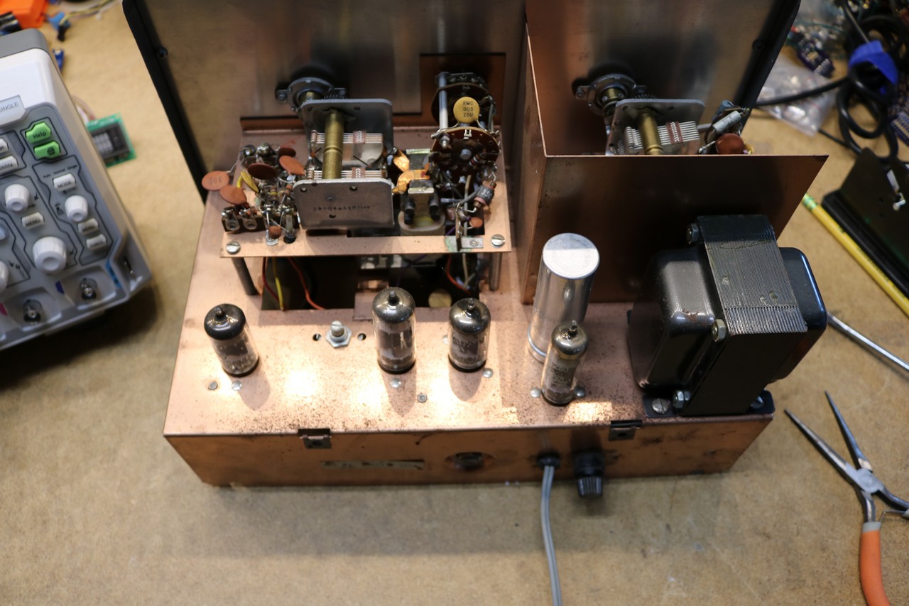
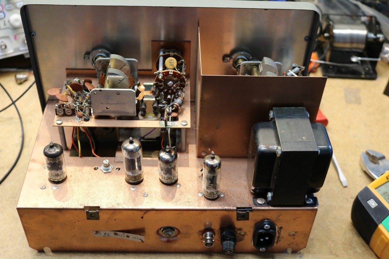
Eico 369 Top Back View

Among the tubes in the above picture is an aluminum cap — that’s the main filter cap. I ended up replacing it because I generally replace all really old electrolytics, even tough it didn’t test bad. Next up is a picture of the Sweep Oscillator Variable Capacitor:

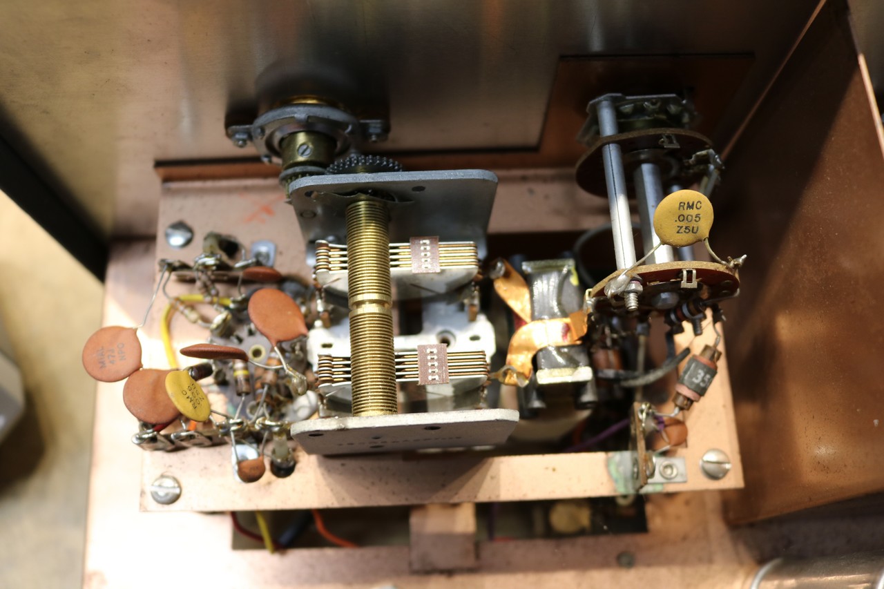
Eico 369 Sweep Oscillator Section

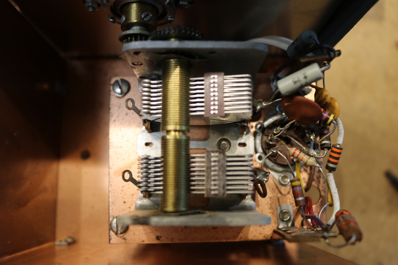
Next up is the Marker Oscillator Variable Capacitor:

Eico 369, Marker Oscillator Section

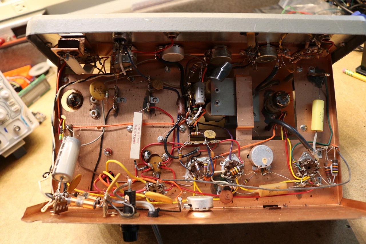
Here is a picture of the underside of the Eico 369:

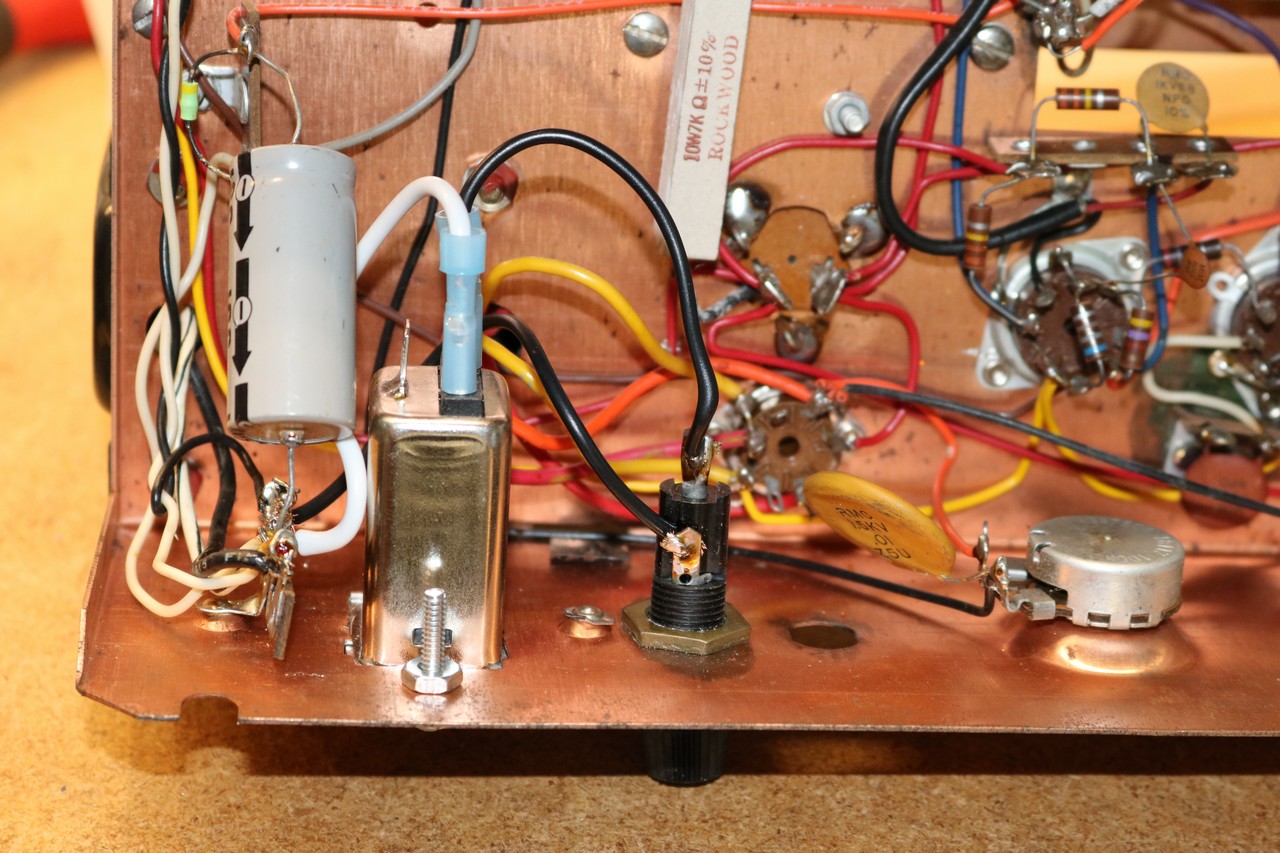
Eico 369, view from below

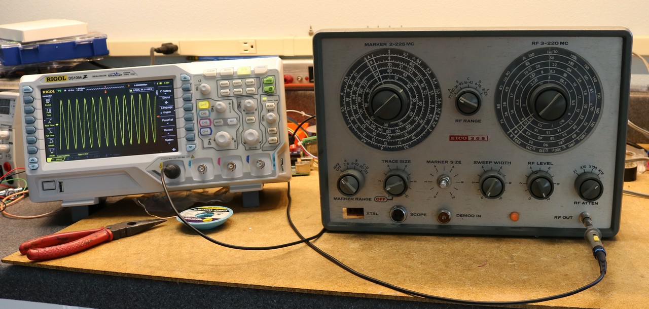
The very first modification I did was to replace the RF output jack with a BNC jack, then I verified I was getting an RF signal using my Rigol DS1054Z:

Eico 369, Checking RF Output with Scope

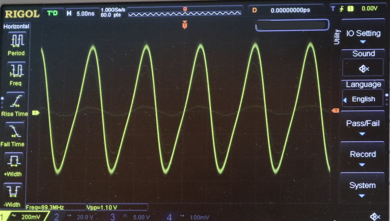
Here’s a closeup of the waveform at 89Mhz:

Eico 369, RF Out, 89 Mhz

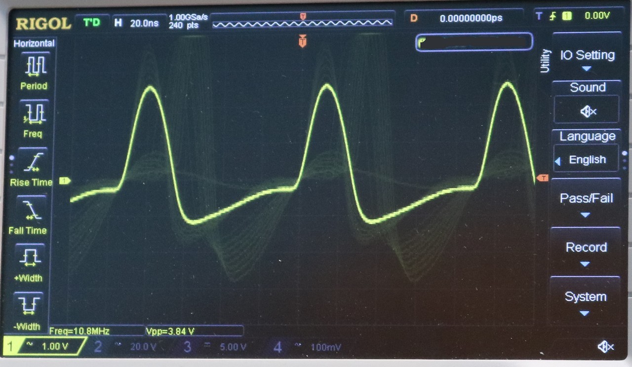
… and here’s one at 10.8 Mhz:

Eico 369, 10.8 Mhz

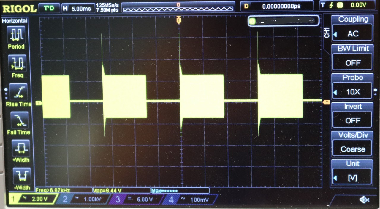
You’ll notice the waveform is not quite sinusoidal. That doesn’t seem to be that uncommon for RF generators of this era and design. However, you’ll also notice if you look closely that there’s a bunch of other dimmer waveforms. This intially had me quite concerned and I went to the antique radio forum for clarification. The Eico 369 has a blanking circuit, that switches the oscillator on and off at 60 Hz, and every time it switches on, it’ll generate a bit of noise. This noise results in those dim waveforms. It looks nasty when viewing the raw RF output, but when you’re actually sweeping it’s not bad, and it’s obvious that the noise is all concentrated at the start of the sweep.

Backing the scope way out, so we can see several blanking intervals, we can understand where the noise is:

Eico 369, Blanking Intervals Showing Noise

Another modification I performed was to remove the old EMI/RFI filtering and old power cord and replace it with a modern EIC receptacle, so I can use any old computer power cord I have laying around:

Eico 369, Power Input Replaced

I also added a BNC jack onto the back that I can use to read the exact freqeuncy of the marker oscillator using my frequency counter:

Eico 369 Modifications - new power recept and marker jack

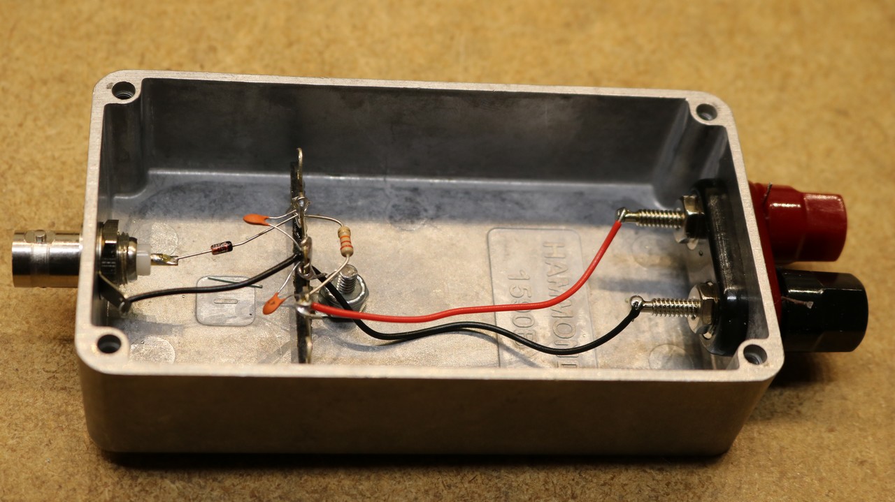
For testing and calibration, the manual suggests you make a ‘broadband detector’. It a germanium diode (I used a 1N60), some caps, and a resistor:

Broadband Detector

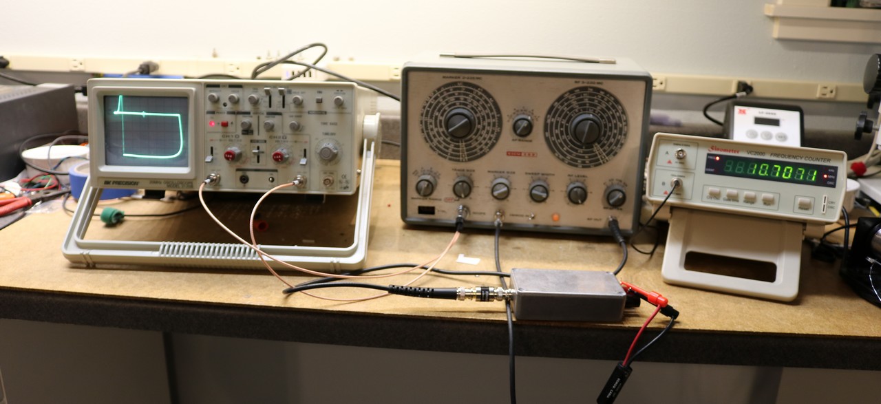
Now that I’ve made the broadband detector, I can finally perform a test sweep. I connect it to my old BK Precision 2120B oscilloscope.

Eico 369, Sweep using broadband detector

Here’s a close-up:

Eico 369, Sweep using Broadband Detector, close-up

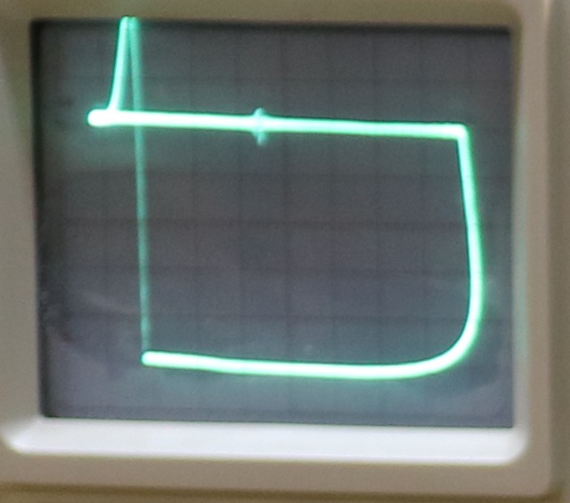
So let’s discuss what we’re seeing above. The topmost horizontal line is the sweep, and it sweeps from left to right. The blip you see right in the middle is the marker oscillator, which is set to 10.7 Mhz. The line is flat because the broadband detector has a flat response curve — it attenuates all signals equally. On the right hand of the display, you scan see where the Eico 369 blanks, and drops the output down to zero. It then sweeps along the zero line back to the left. The blanking circuit disengages, and we get that big noisy spike that you saw before, and then the sweep begins over again.

All things considered, for a piece of vintage test equipment, this thing is pretty fun to play with, and is a useful addition to the bench.

Aoyue 128 Soldering Tip Polisher Review

$
0
0

Unable to resist yet another gadget, I bought a soldering tip polisher. Someone please save me from myself…

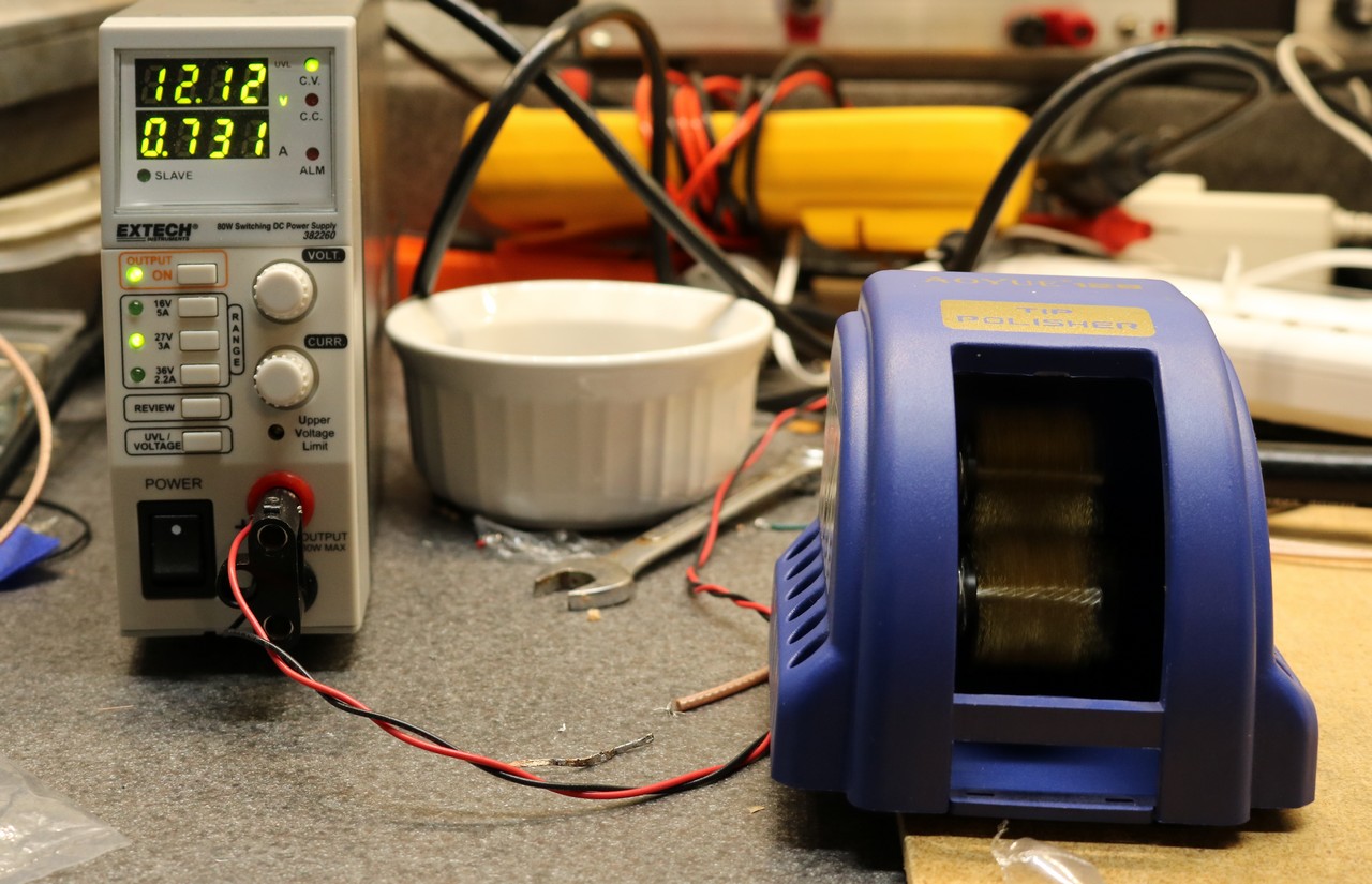
The tip polisher costs about fifty bucks. There’s a lot of plastic in the construction of the product, but it seems to work. It has two rotating brushes, driven by a small belt and a 12VDC motor. Some high resolution pictures of the tip polisher are shown below:

Aoyue 128, connected to my PSU to measure power consumption

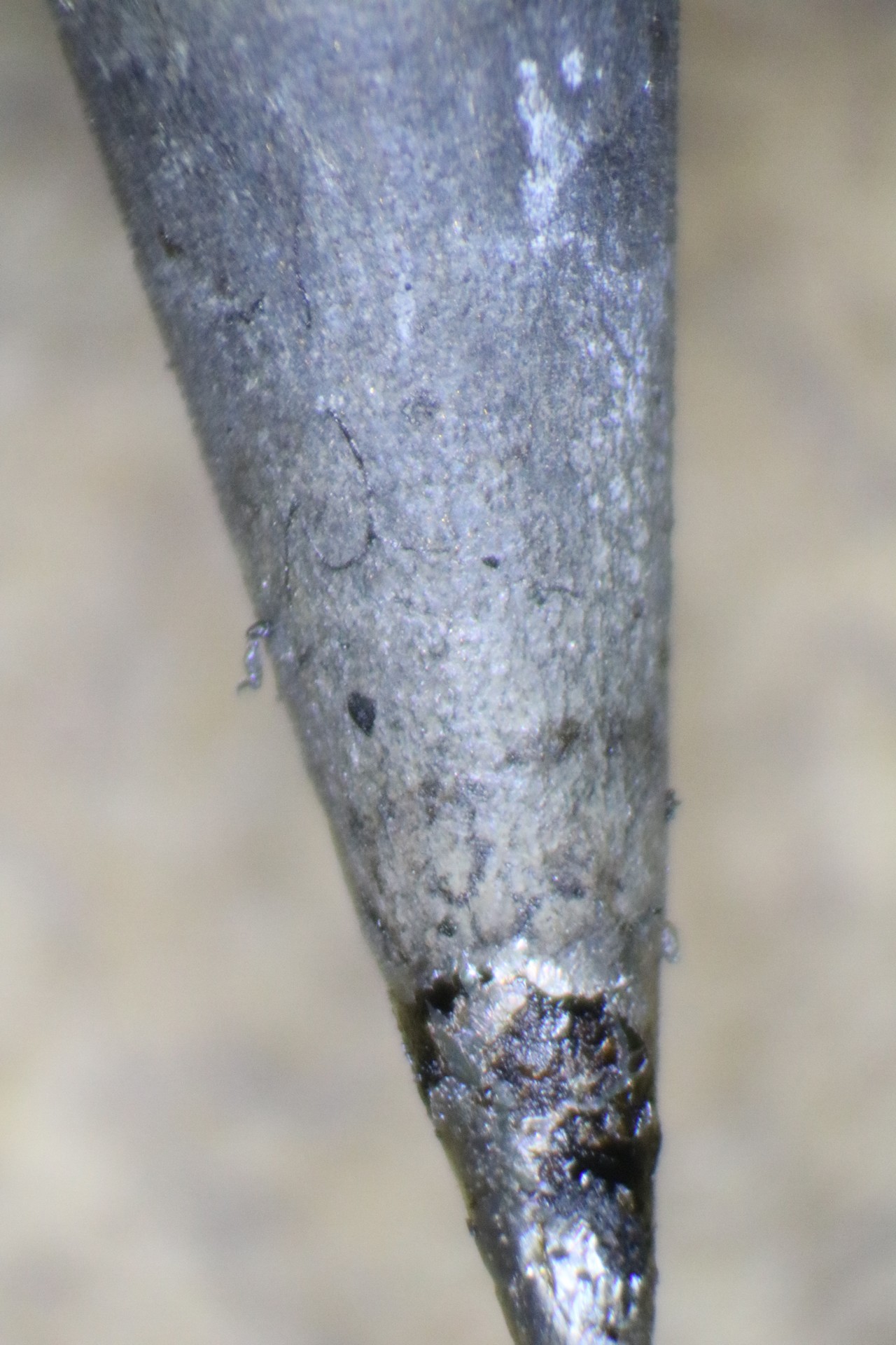
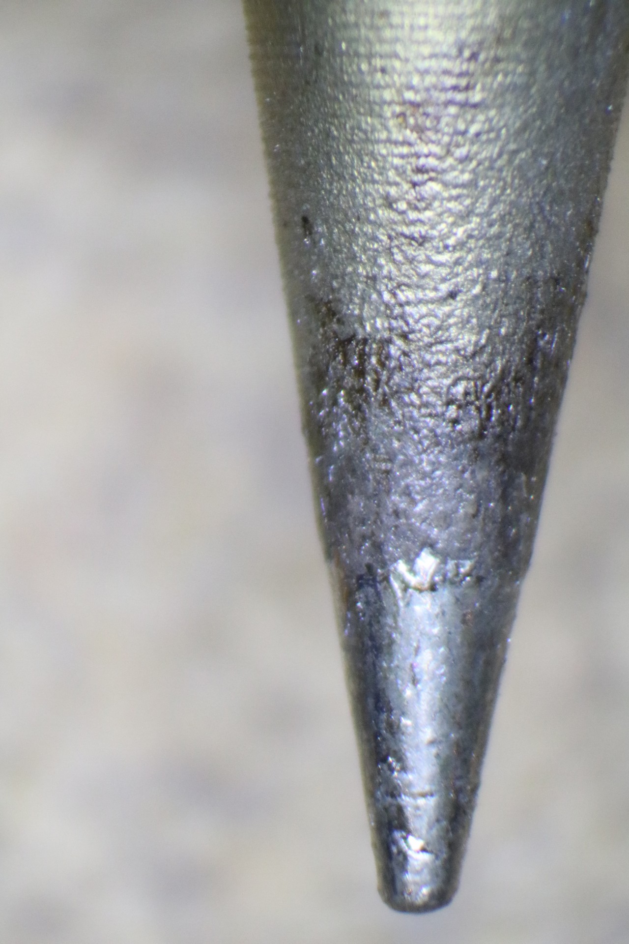
Here’s some pictures of me cleaning my soldering iron tip:

Soldering tip, before cleaning

Soldering tip, after cleaning and plating

As you can see, it did a decent job of cleaning up what was a fairly cruddy soldering iron tip. The motor draws about 730ma while free running, or about 950ma if I stall it by shoving my finger into the brushes. The included 2A switching power supply should be sufficient.

Would I buy it again, if I had it to do over? I suppose so. It’s not an expensive tool, and it does do a reasonable job of cleaning the tip.

Sparkfun third hand kit – review and modifications

$
0
0

I’ve always wanted a sparkfun third hand kit, so I bought one on Cyber Monday:

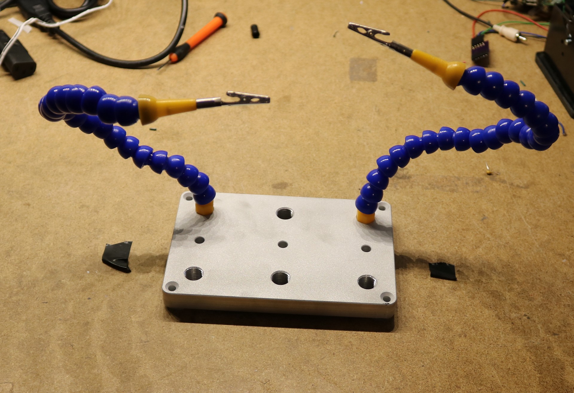
Here’s a still shot of the third hand kit as assembled:

Third Hand Kit, assembled

The first thing you’ll notice is that the alligator clips are really small, as compared to my old Radio Shack Third Hand kit. I do a pretty good job of showing the relative size comparison in the video. Bigger clips would have been nicer. My other criticism is that I find the alligator clips don’t rotate all that well. One of the nice things about the old Radio Shack Third Hand is that the clips would rotate smoothly and the joints would pivot smoothly.

The base plate is really well done, a total of six threaded spots for attaching the flex arms (you can buy additional flex tube kits from Sparkfun). There’s also countersunk holes for screwing it down to your workbench if you wish to do so.

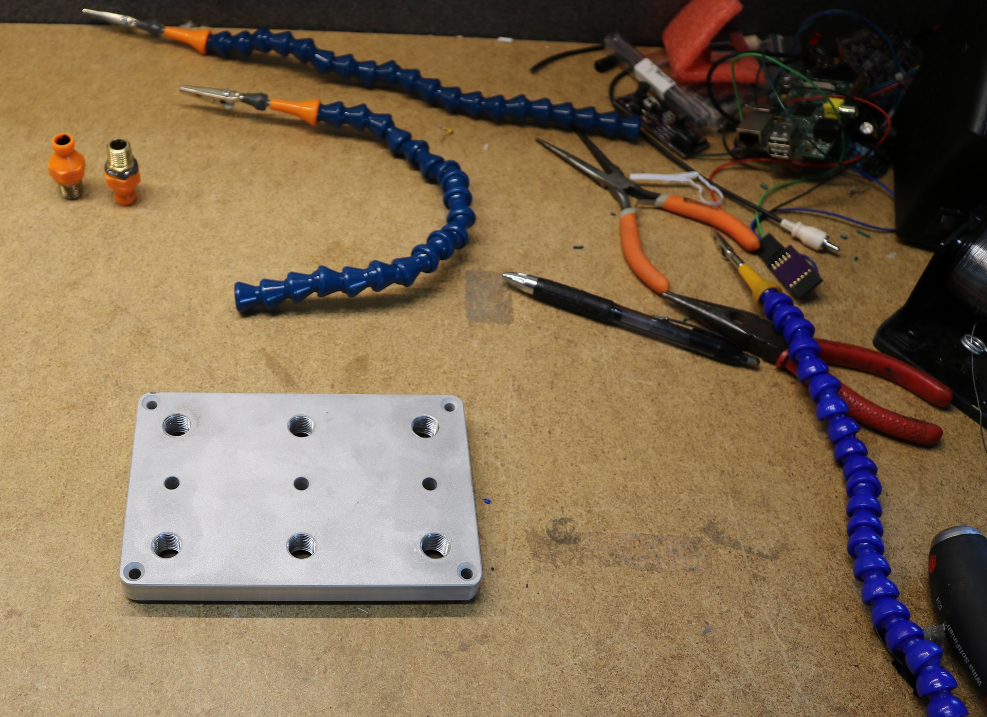
The flex tubes are what people in the machine industry would often call “Loc-Line”, though Loc-Line is a particular brand name. The stuff used in the spark fun kit is a different brand. The balls and sockets are a slightly different size than name brand Loc-Line, and are not quite compatible. I had some Loc-Line on hand, so I compared the two. I felt that the Loc-Line may have a little smother pivot action. Also of note is that the name-brand Loc-Line is a darker shade of blue than the tubes that came with the Sparkfun kit:

Name-brand Loc-Line on the top, off-brand on the right

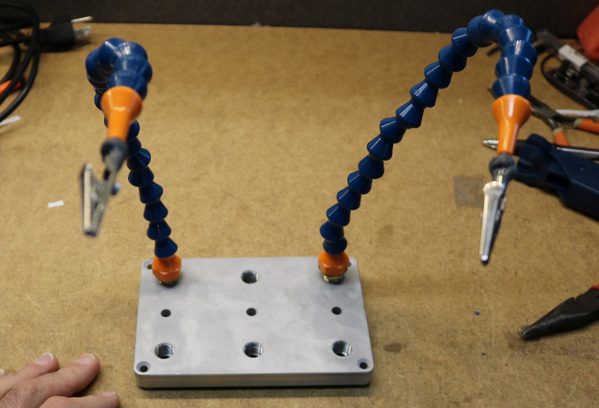
Since I had some name-brand Loc-Line on hand, I decided to make two new flex arms using the name brand Loc-Line and larger alligator clips. To attach my alligator clips, I JB-Welded some 8/32 nylock stop nuts onto the ends of them. The nylock nuts have just the right amount of friction for smooth rotation. The holes tapped into the aluminum plate were not the 1/4 NPT that I needed to attach my Loc-Line, but were instead metric 14×1.25. The sizes were quite close and it was easy to re-tap them using a tap and die set.

Modified third hand kit

My “hack” lasted about two days and then broke. It turns out JB Weld has excellent compressional strength and sheer strength, but lousy tensile strength. If you make a JB Weld butt joint, you can snap it fairly easily. The material is a lot like concrete in that respect, and one will notice that they often add concrete to rebar. So I remade my alligator clips and added some ‘rebar’ in the form of a few chunks of 24ga solid wire to the epoxy. It hasn’t snapped again.

Eico 430 Oscilloscope

$
0
0

I can’t resist buying vintage test equipment:

The Eico 430 is a tube-based oscilloscope. By that I don’t simply mean that it uses a Cathode Ray Tube, but that it uses vacuum tubes for the amplifiers and oscillators as well. It’s truly an amazing piece of equipment for the era that it was created in. The video above walks through my trying out the scope (it didn’t work right… does anything bought on ebay ever work right??) to me fixing the scope, and then using it in conjunction with a couple RF frequency generators and my sweep generator.

Now for some still shots:

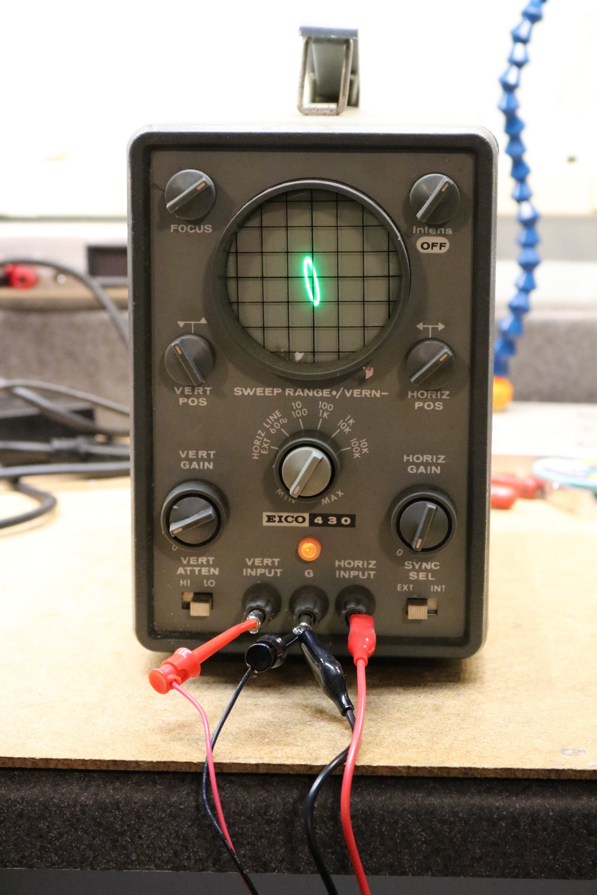
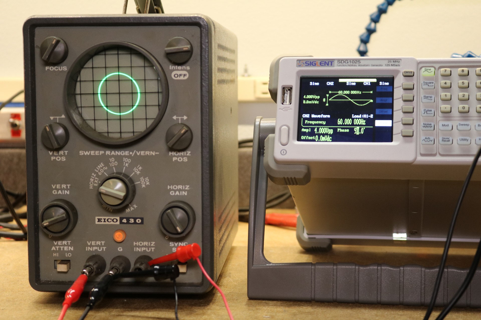
Eico 430 Tube Era Oscilloscope

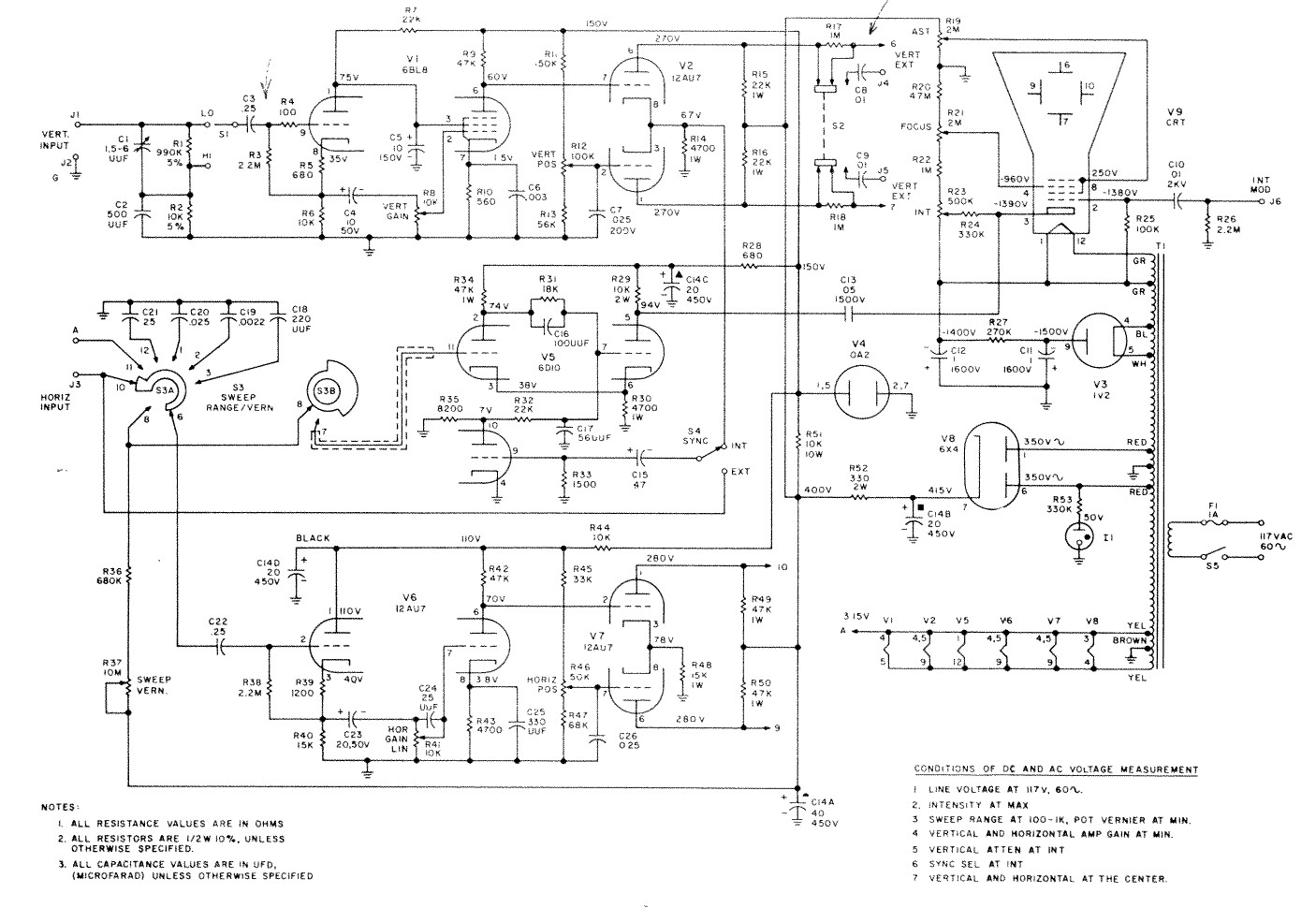
It’s probably not evident from that picture, but the scope isn’t actually working very well. The Horizontal gain control is fully clockwise, and there’s less than one division of horizontal deflection on the lissajous pattern that I’m displaying. I noticed the gain would improve at higher horizontal frequencies, and I decided to take a look at the schematic:

Eico 430 Schematic

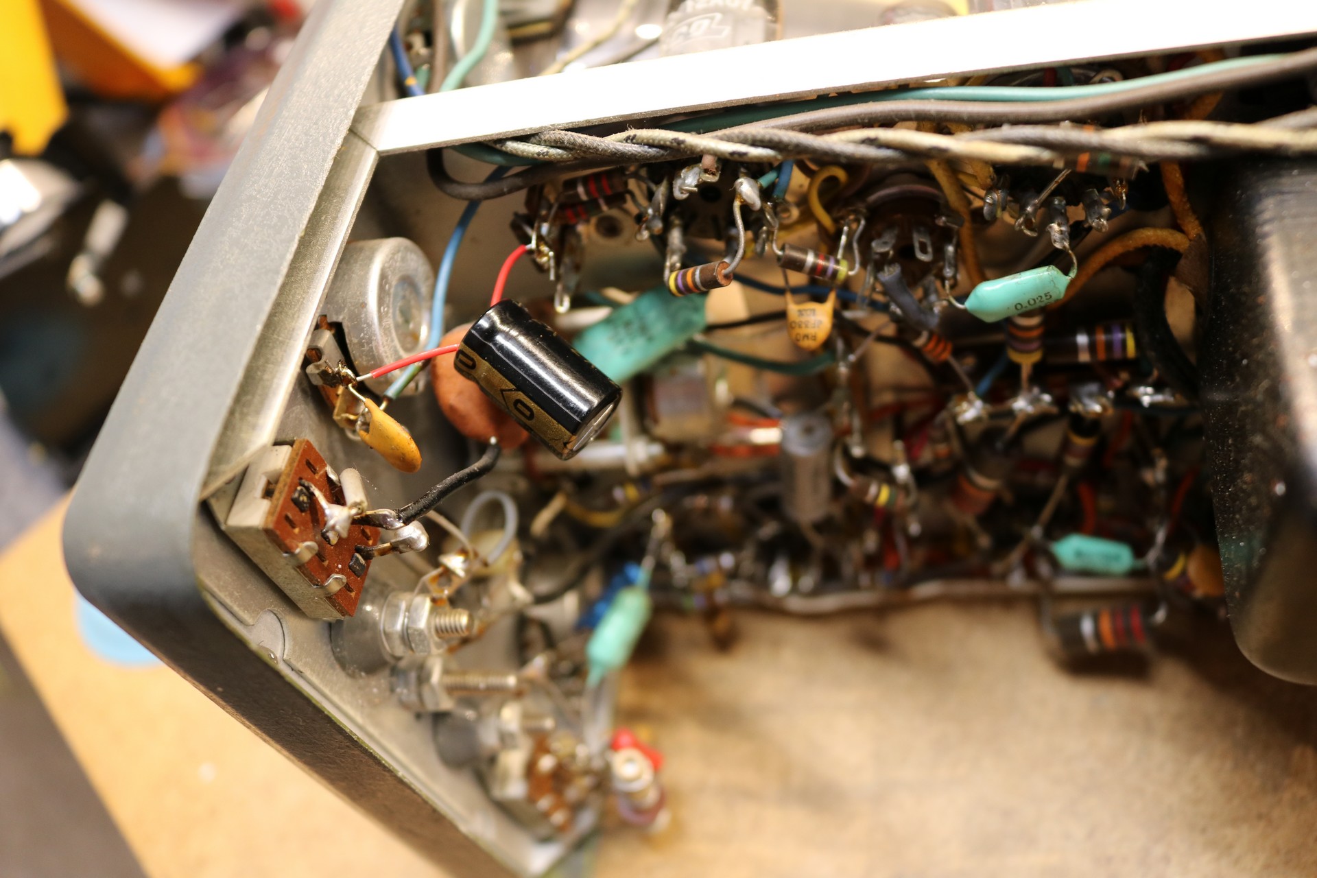
I was immediately suspicious of C23, a 20 microfarad electrolytic capacitor connected to the horizontal gain capacitor. It’s an electrolytic capacitor that appeared to be original, and the attenuation at low frequencies would be consistent with a failed capacitor. I replaced it with a modern cap, and the problem was fixed:

Eico 430, lassajous pattern after capacitor fix

Here’s a picture of the replacement capacitor:

Eico 430, replacement capacitor

Well gee that turned out to be really easy. The scope works pretty well. I bought it with the particular purpose in mind of using it in X-Y mode in conjunction with a sweep generator, and that’s shown in the video at the top of this post.

Now for some teardown images:

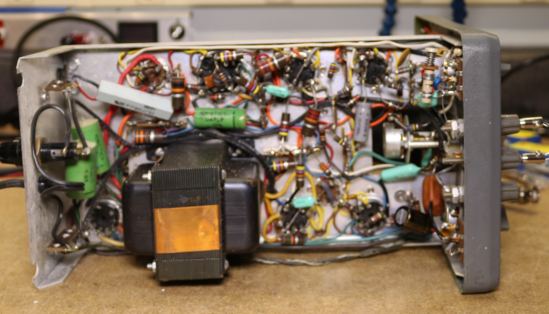
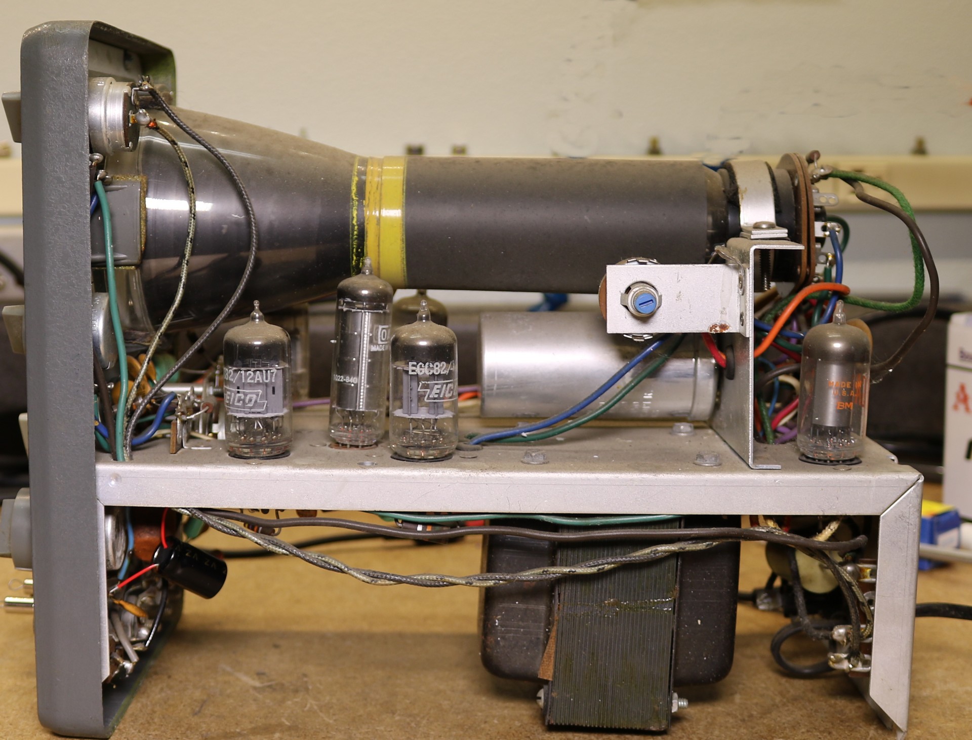
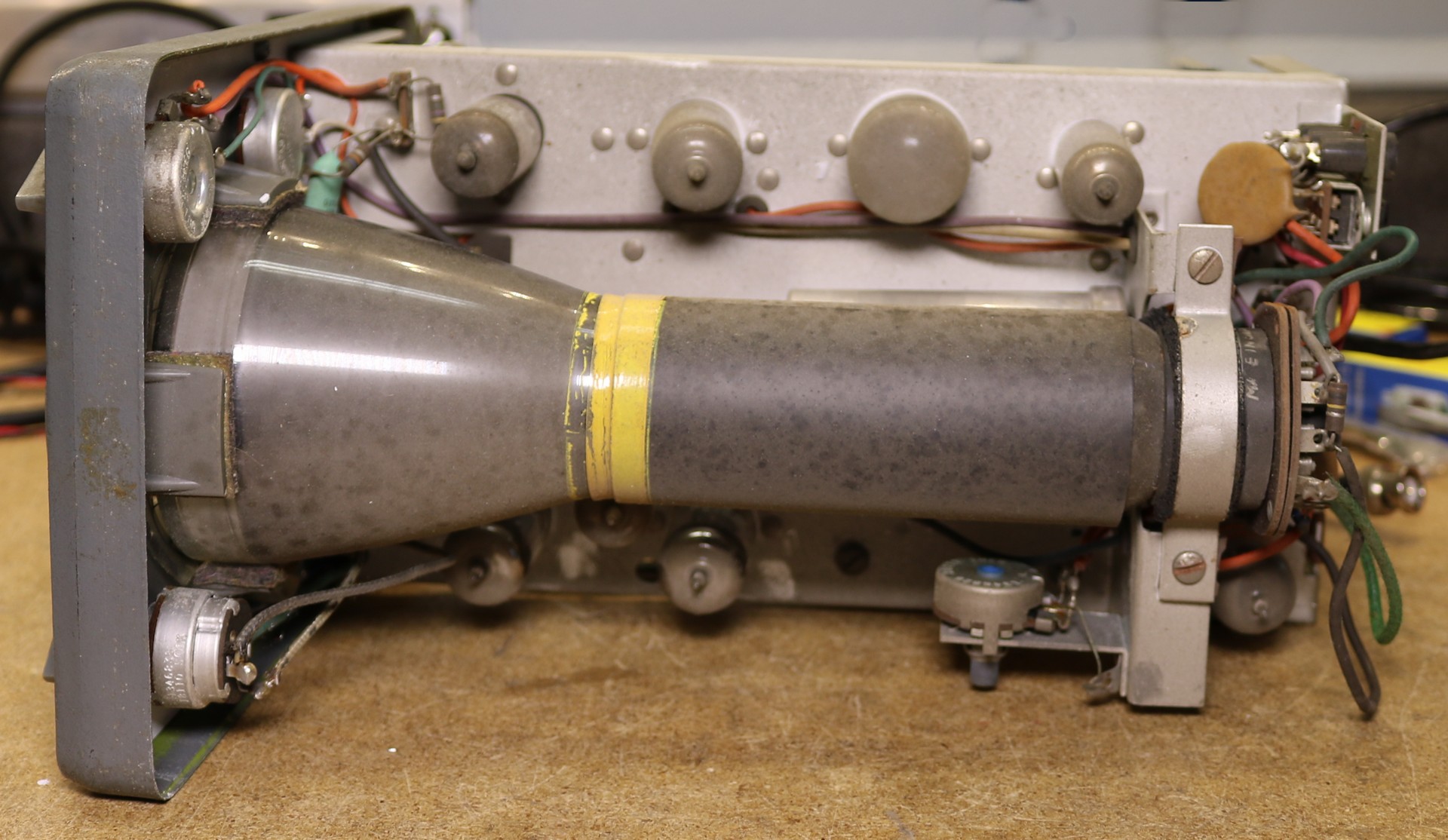
Eico 430, view from underneath

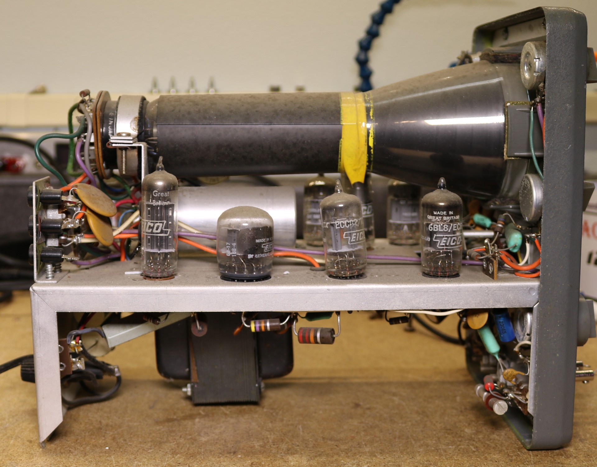
Eico 430, Left View

Eico 430, right side

Eico 430, top view

As far as vintage gear goes, a vintage oscilloscope is one of the funner pieces of gear that you can acquire. Just beware that you might have to repair it yourself!

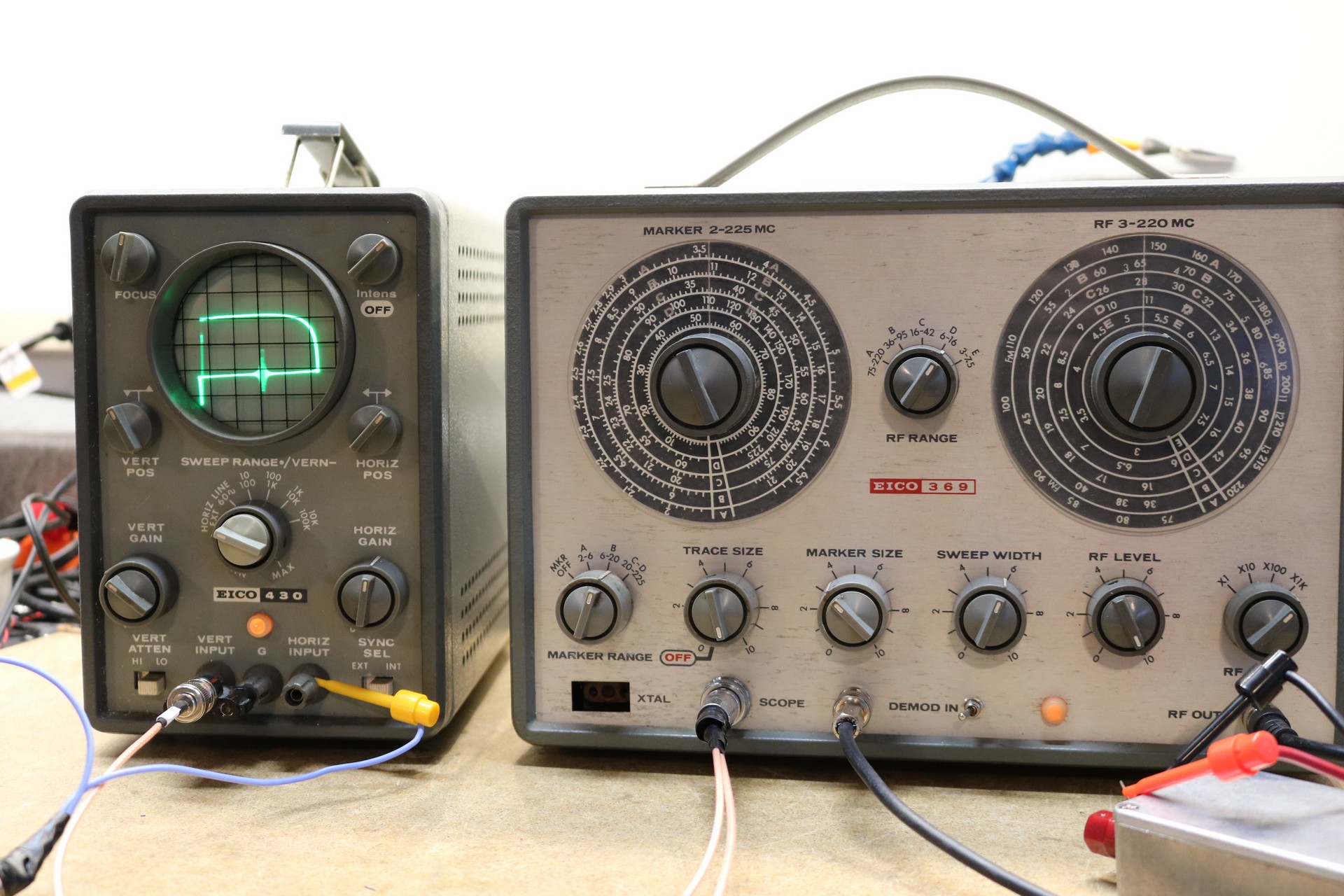
Here’s a picture of my Eico 430 in action, together with an Eico 369 sweep generator:

Eico 430 oscilloscope with Eico 369 Sweep Generator


Raspberry Pi Switching Power Supply Shield

$
0
0

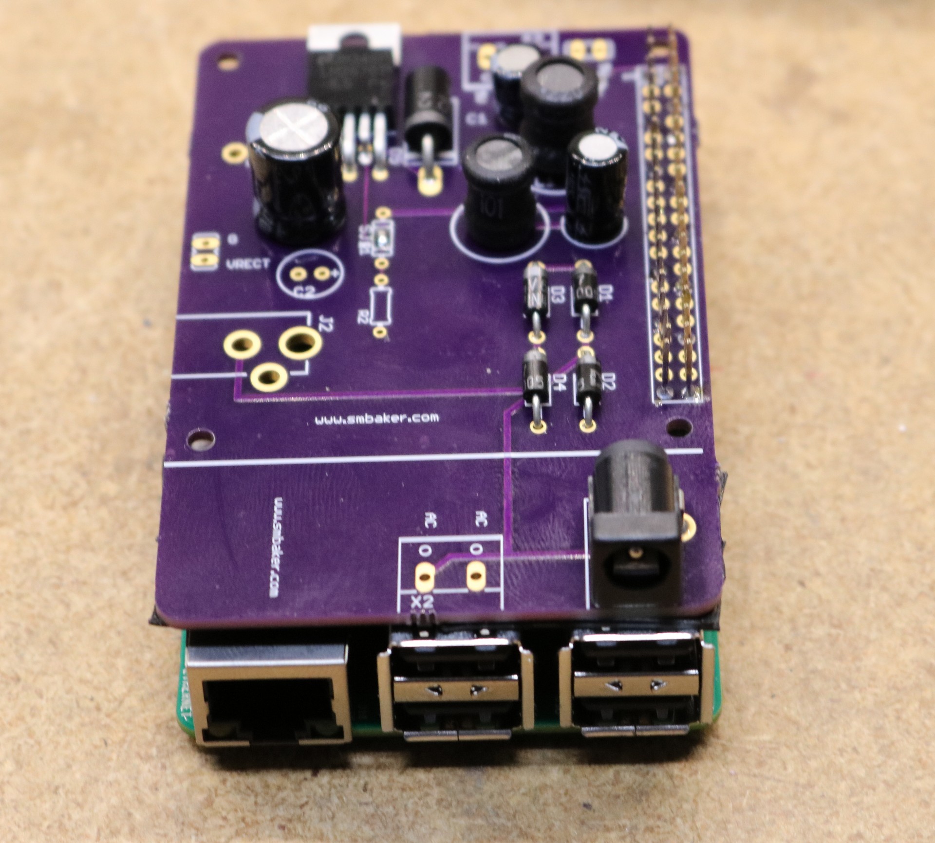
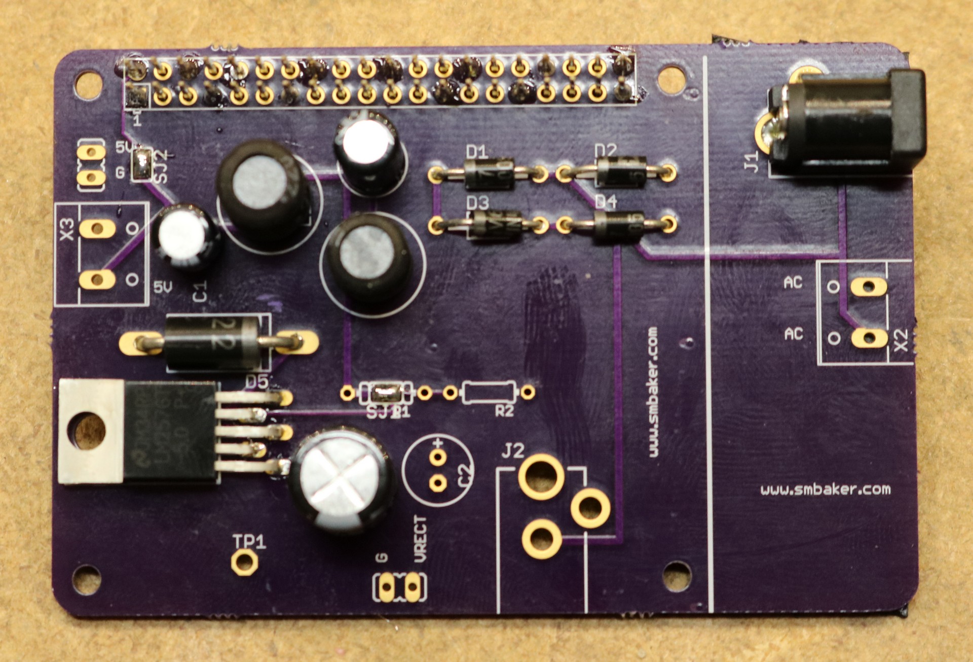
I like to power my projects from 12V, and the Raspberry Pi only natively supports 5V. Often I’ll add a small switching power supply to my designs to accommodate this. I finally got around to making a supply in the form factor of a shield (I’d call it a “hat”, but technically I believe a “hat” requires a configuration eeprom). Here’s the result:

Raspberry Pi Power Shield

As you can see, I’ve designed it so that the power jack can be placed in either of two locations, one of them right on top of the ethernet and USB ports, which happens to correspond with the back panel location of many of my projects. I’ve also made provisions for terminal block power input. There’s a full-wave bridge rectifier, so it can be plugged into AC. There’s an output header for 5V out as well as a terminal block for 5V out, so it can be used to power external electronics as well. The white line shows where the board can be cut, to discard the portion that overlaps the USB and Ethernet ports, if desired.

It might not be obvious from the image, but I used a stacking header so all of the GPIO pins are still usable. Only two of the Raspberry Pi pins are connected to — 5V and ground. I only soldered enough of the header to the PCB to make it mechanically sound.

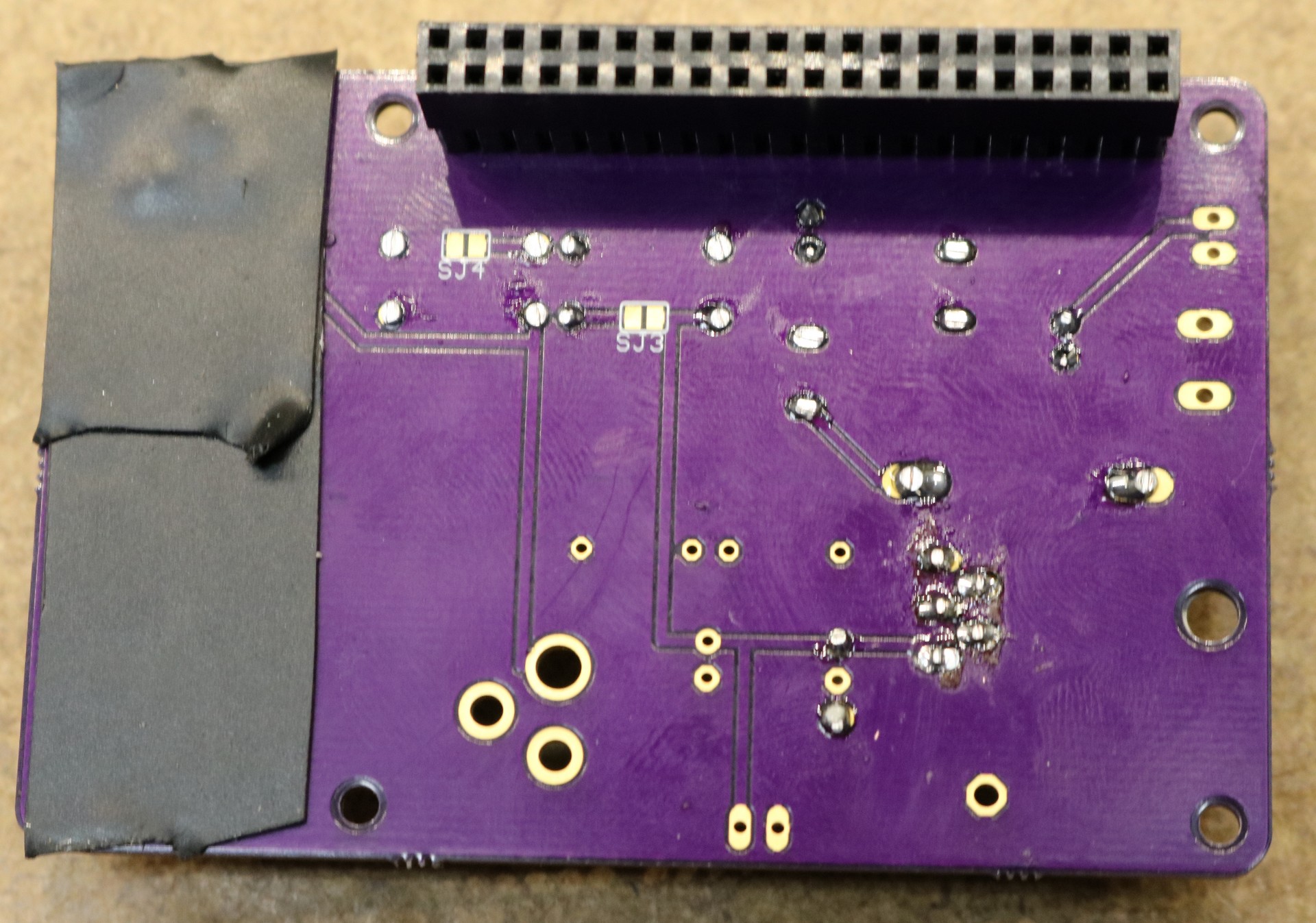
When overlapping the Ethernet / USB ports, I added some thick black tape, just to make sure the bottom of the power jack doesn’t short against the ethernet / USB ports. The next revision, I’ll have to consider using a SMD power jack instead.

Power Shield, under side

Here’s a picture of it mounted on top of a Raspberry Pi 2:

Power Shield mounted to Raspberry Pi 2

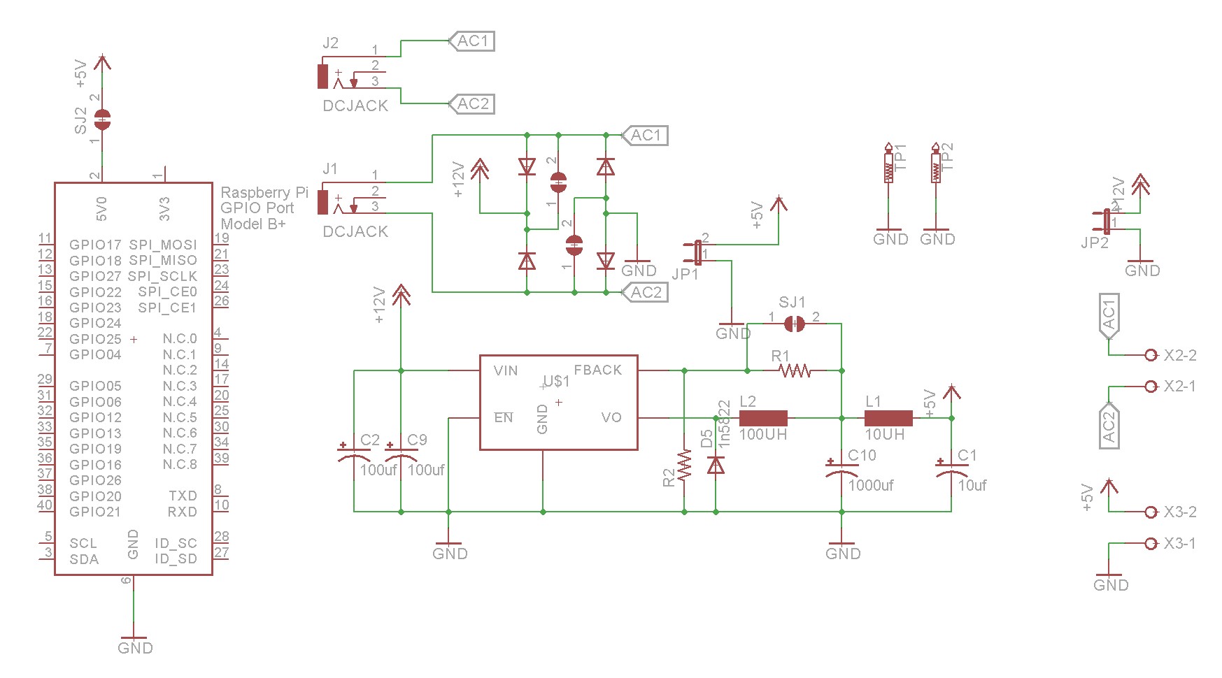
The schematic is right out of the data sheet for the LM2576 switchmode regulator:

Power Shield Schematic

DIY Nixie Tube Frequency Counter

$
0
0

In this video, I build a Nixie Tube Frequency Counter. I’ve always wanted a Nixie Tube Frequency Counter, but never did find one on eBay that really jumped out at me… So I just decided to go ahead and build my own. My goals were:

  • Nixie Tube Display
  • Range from a few hundred Hertz to a couple of Gigahertz
  • Sensitivity to 5oomV
  • Six significant digits

Accuracy is something that I haven’t put a whole lot of thought into. I do have some TCXO (temperate compensated crystal oscillators) on hand, and some propeller boards on order to use them. Once I get the boards on hand, I’ll see if I can build up a version of the counter with verifiable accuracy.

The CPU

For a CPU I chose the Parallax Propeller. Many of my other projects have used the Raspberry Pi lately, but when it comes down to realtime programming, I like the prop. It’s easy to implement a deterministic realtime loop in one of the cogs while using the other cogs for other tasks, such as operating a display or user interface.

In building the prototype I first used a Parallax Propeller Professional Development Boar (PPDB), and then switched to a Propeller Proto-Board. There’s very little that needed to be done in the way of digital work — the counter signals basically come in on a couple of pins and the display data goes out via I2C to my nixie driver boards.

The Nixie Driver Boards

I used the same boards that I used for the Nixie Tube Calculator project, also described in an article and video of mine called ‘Controlling Nixie Tubes via I2C’. Basically the way these boards work is to use K155D Nixie Tube drivers controlled by I2C IO Expanders (MCP23017 and PCF8574). These boards can be daisy chained to control up to 32 Nixie Tubes. I only needed 8 tubes for this project, controlled from two of my Nixie Display modules. The modules also allow control of the decimal point, and there’s even a provision for LED backlighting.

The tubes I selected are the popular IN-12. They’re quite easy to obtain on eBay, cheap, and are easily socketed to a pcboard. Also available are the IN-15A and IN-15B which display a variety of symbols. The IN-15A allowed me to display “M” or “K” (for megahertz and kilohertz, respectively) and the IN-15B allowed me to display a “Hz”. Yes, I did waste tube budget on a tube that I only use to display the “Hz” symbol and nothing else.

Power Supply

I use a variant of my HVPSU, described elsewhere in my blog. It’s a TL494 boost converter that outputs around 160V to light the tubes. Also present on the power supply board is a 5V switchmode power supply to power the propeller proto board.

Lo-range front end

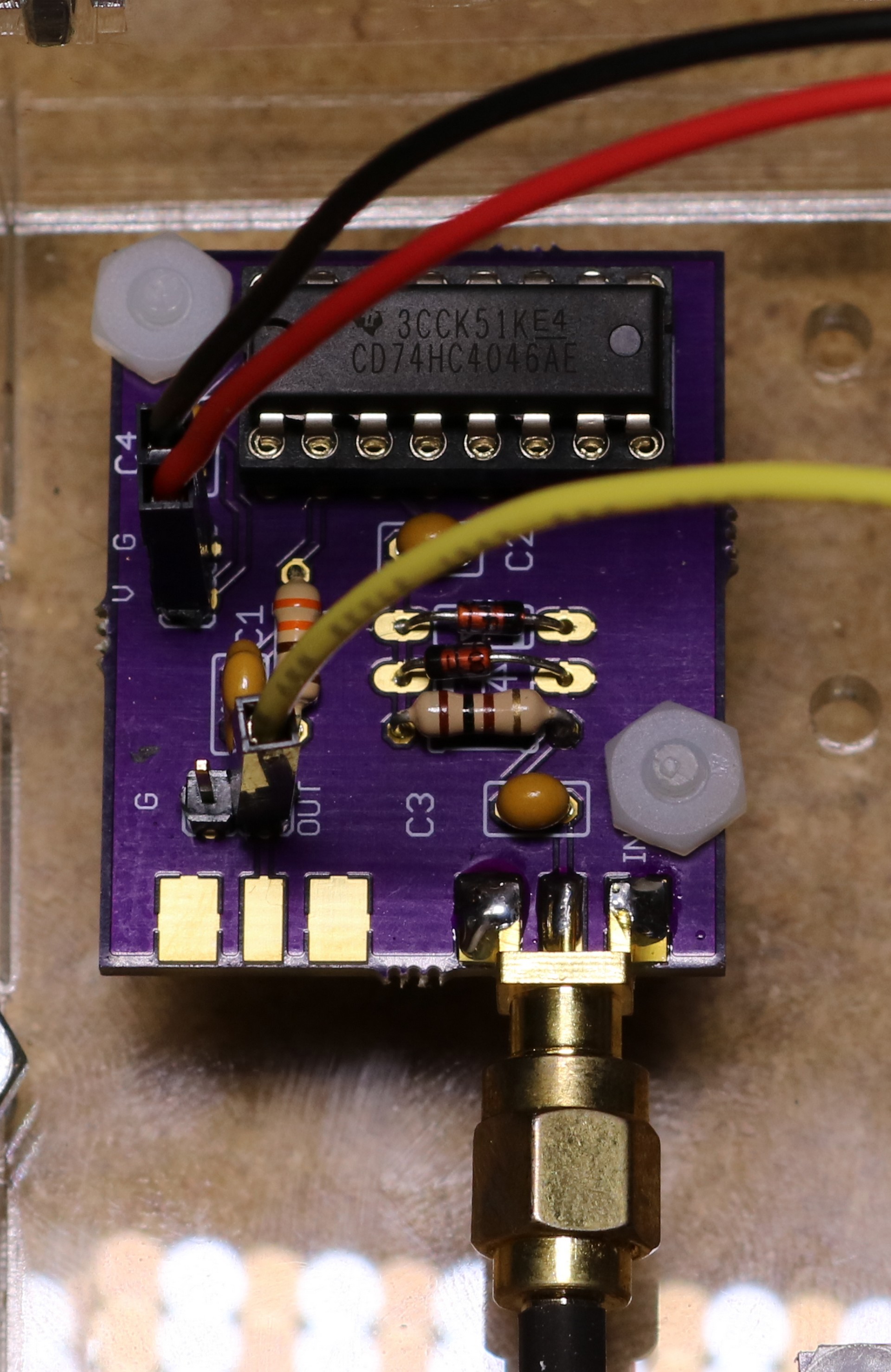
My first attempt to build a frequency counter had me connecting my function generator directly to the propeller. That worked fine for square waves, but failed miserably for sine waves. I quickly learned that I need some kind of a front end to condition and amplify the signal. Scouring the Internet for design ideas, I found the 74HC4046 chip. The 75HC4046 is a phase locked chip, but it has a nice signal amplifier built in. Here is a picture of the breakout board that I designed:

Lo-range frequency measurement using 74HC4046

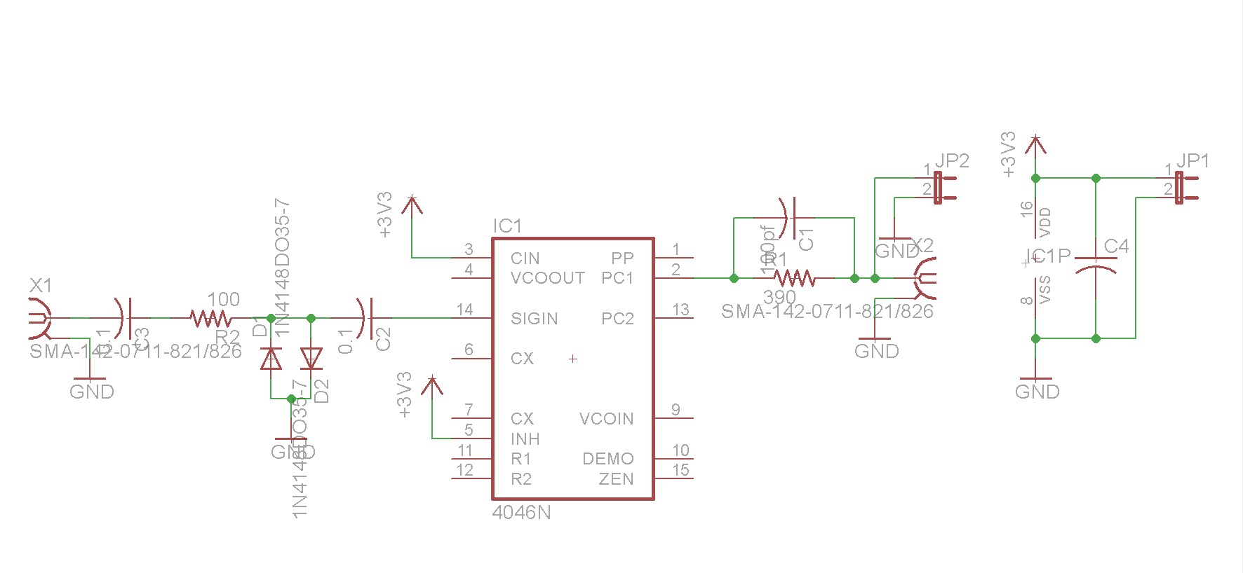
Schematic of the breakout board:

74hc4046_breakout board schematic

I was able to get the Propeller to count the output of the 74HC4046 directly to about 32 Mhz. We could probably get a bit more out of the 74HC4046 by adding a frequency divider and using the prop to count the divided frequency, but we’re not going to make it anywhere near our Gigahertz goal with that approach. So it’s time to develop a hi-range front end.

Hi-range front end

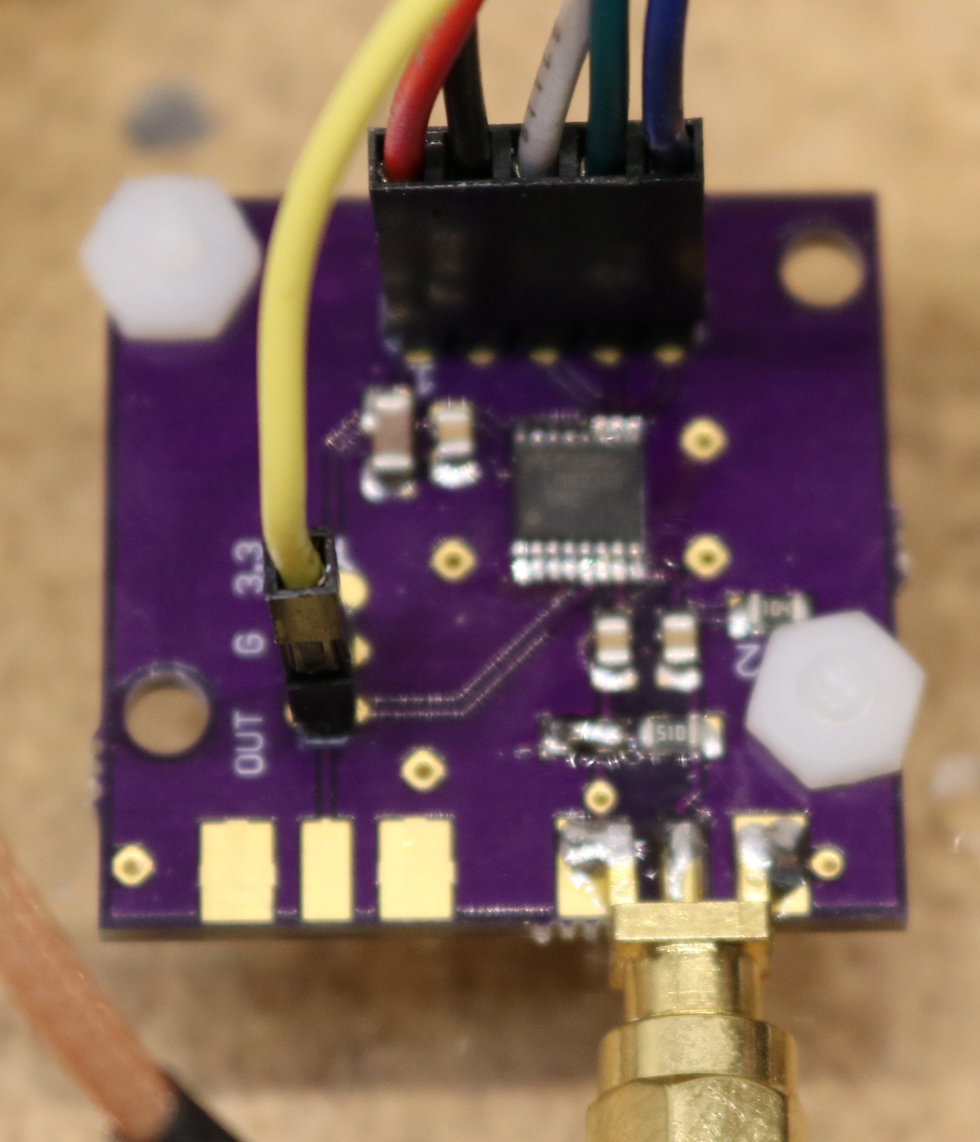
For the hi-range, I wanted to be able to get from 25 Mhz to a couple of Gigahertz. Again, scouring the Internet I saw some people using an LMX2322 prescaler in their designs. Like the 74HC4046, this thing is intended for phase locked loop applications, but we can get away with just using the detector and prescaler functions. It’s controlled via a serial interface that lets you configure the prescaler.

Configuring the prescaler is a bit weird, and took some time to figure out. It’s a 32/33 prescaler. It takes a pair of numbers, A and B, and it divides the input frequency by 33 A times, and then divides by 32 (B-A) times. It also has the restriction that B must be greater than or equal to 3.

So let’s take a simple example. Let A be 0 and B be 3. This is the minimum values that we can use. It’ll divide the input signal by 33 zero times, and then divide by 32 three times. This yields a divide-by-96 function. I ended up going with A=0, B=4, which yields a divide-by-128 function. Thus when there’s a 1 Ghz input signal, the LMX2322 will output 7,812,500 Hz. We just have to multiply our measured frequency by 128 to get our display value.

hi-range front end using lmx2322

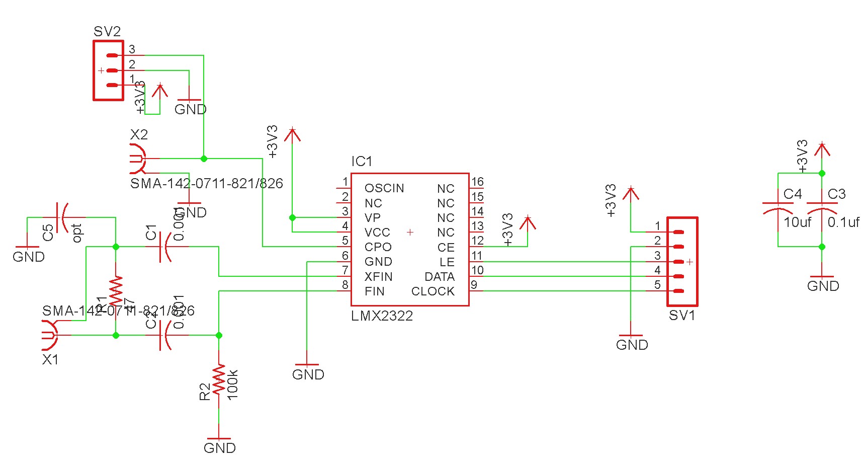
Schematic of the breakout board:

lmx2322_breakout board schematic

Initial Prototype

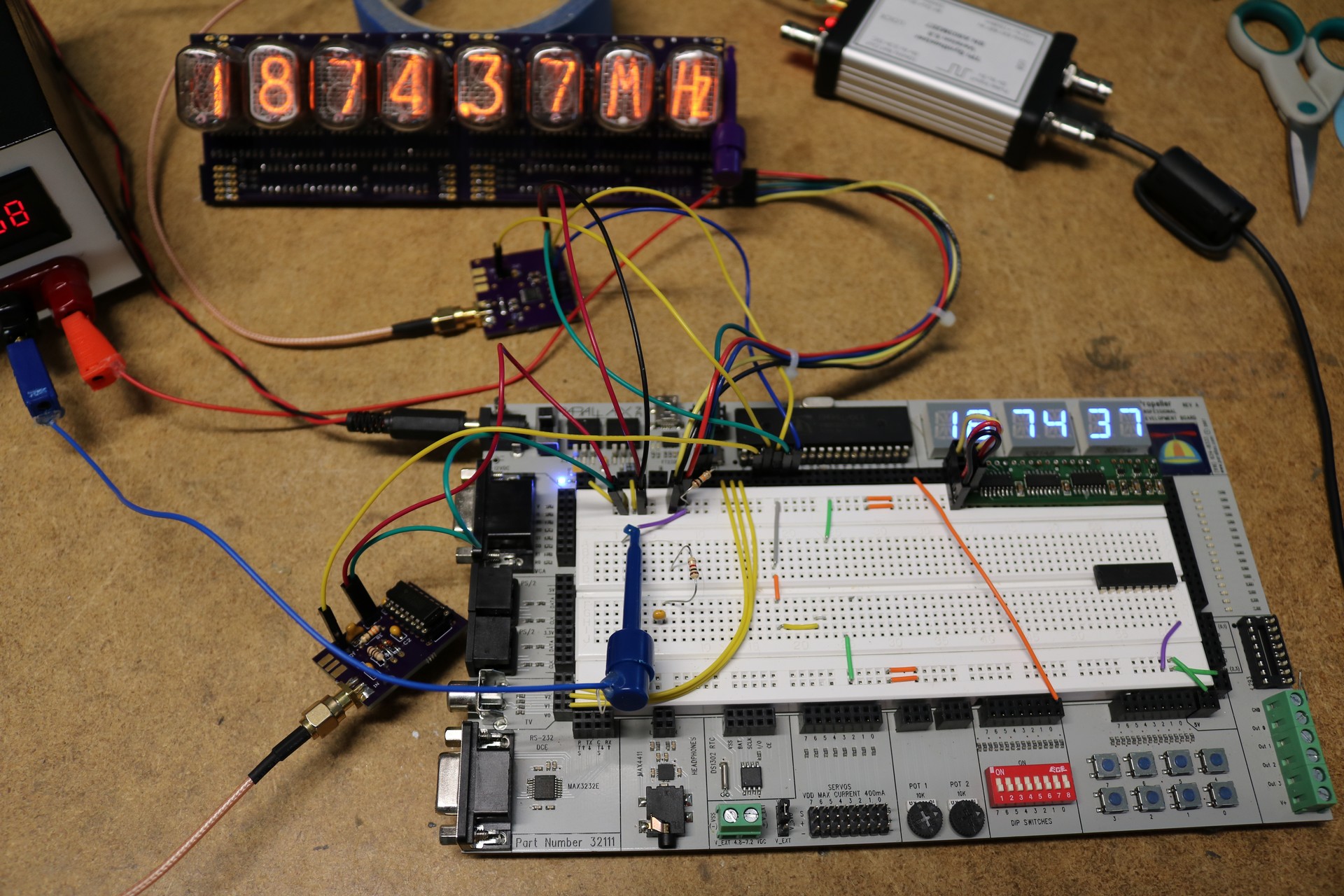
The initial prototype I constructed using a parallax professional development board:

Frequency counter, initial prototype

Final Assembly

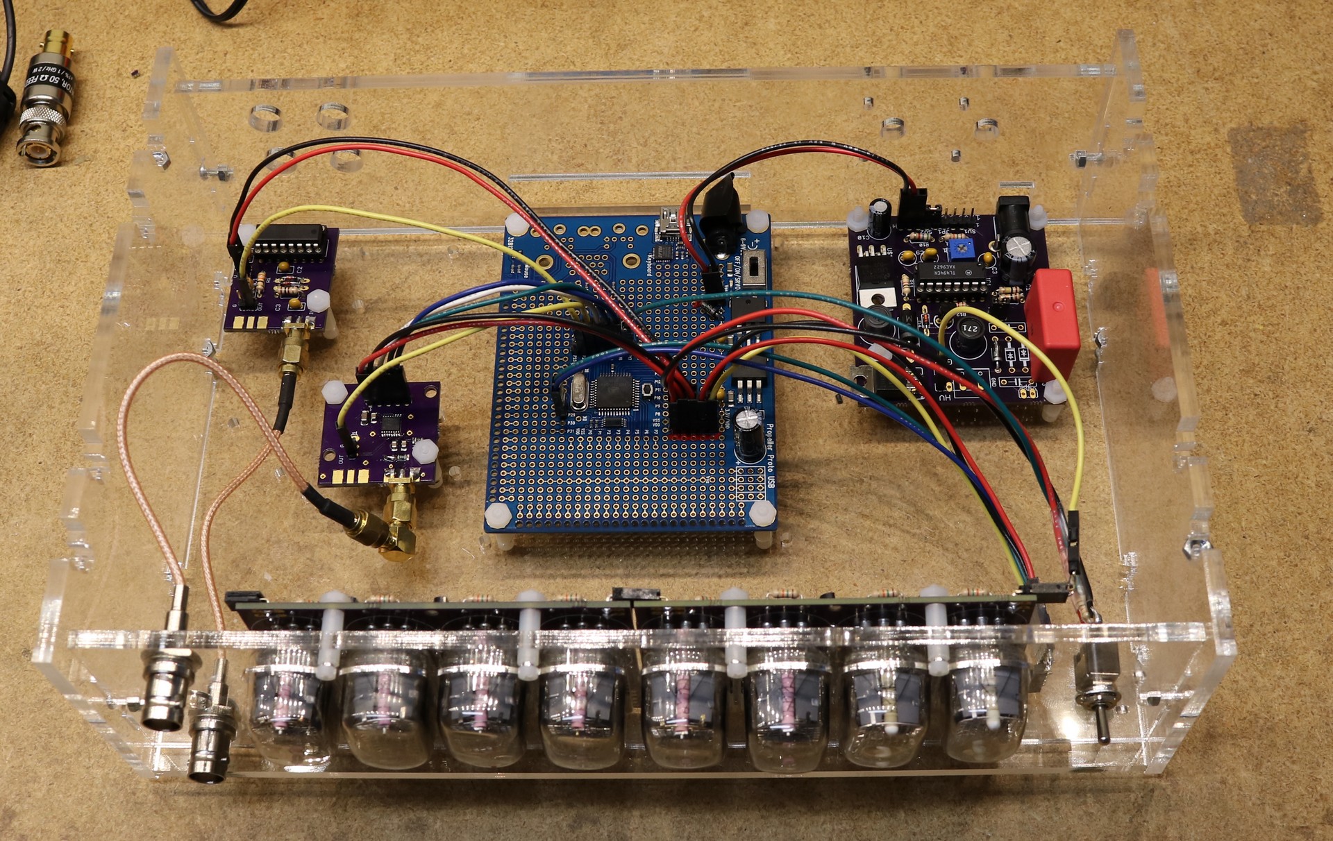
I designed a case, had it laser cut at Ponoko, and fitted the components to it:

Frequency counter components mounted in case

Greater accuracy

The accuracy of a standard crystal isn’t really greater. There will be about a 50ppm manufacturing variation plus there will be variation of the overall oscillator circuit with temperature. To get a reliable frequency reference, it makes sense to use something called a Temperate Compensated Crystal Oscillator. You can get 5 Mhz TXCOs on ebay for about $15. Expensive, but it’ll get you an accuracy of 0.5ppm and compensation for temperature.

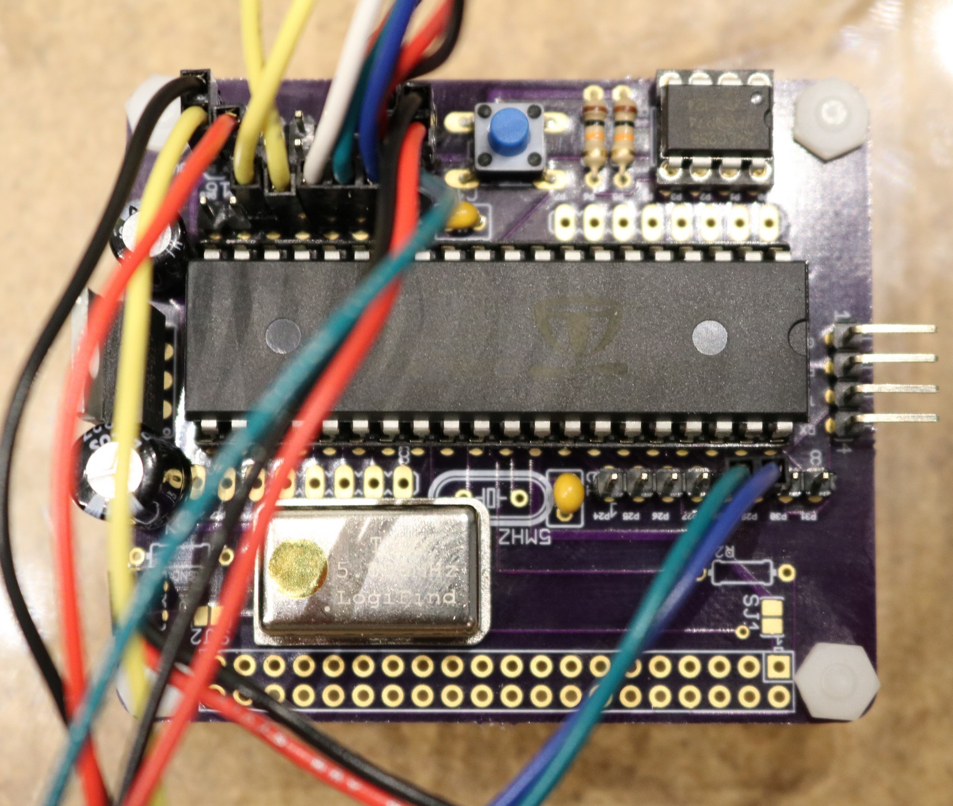
To use the TXCO with the propeller, remove the existing crystal and wire the TCXO’s output to the propellers XI input. The prop’s XO output remains disconnected. I made a custom PCB that mounts a 40-pin propeller, eeprom, TCXO, and voltage regulator. The board replaces the propeller proto-board in the above pictures. Here is an image of the new board. The TCXO is the big metal can:

Parallax Propeller with TCXO

Alternative Hi-Frequency Front End

There were two problems with the LMX2322 as implemented in the project: 1) it topped out somewhere around 1.9 Ghz, and 2) Sometimes it wouldn’t get setup properly over the serial connection to the propeller. I decided to move to a different hi-frequency frontend, the MB506. The MB506 can be configured to divide by 64, 128, or 256. This eliminates to dink around with any serial communication between the prop and the chip. It also seems to function reliably up to about 2.44 Ghz. The problem with the MB506 is that it doesn’t output a nice IO-compatible square wave like the LMX2322 did. It outputs an annoying 1.6 Vpp, centered on ground. I tried a few tricks like using pullup resistors and transistor drivers, but ultimately I decided the safest bet was to just feed it into a second 74HC4046. The resulting schematic is shown below:

MB506 Prescaler

A new PCB is on the way. I’ll update this post when it arrives.

Source Code

The source code is available on my github repository at https://github.com/sbelectronics/prop-freqcnt

Magic Eye Tube interfacing with a Raspberry Pi

$
0
0

This blog post has two videos. In the first one, I bought a magic eye tube kit from eBay for about eight bucks, and I try it out:

In the second video, I use an op-amp that allows me to convert a positive control signal (such as output from a DAC) to the negative grid control voltage (0 to -15 V) needed to control the tube, and then I interface it to a DAC and a raspberry pi:

Basics

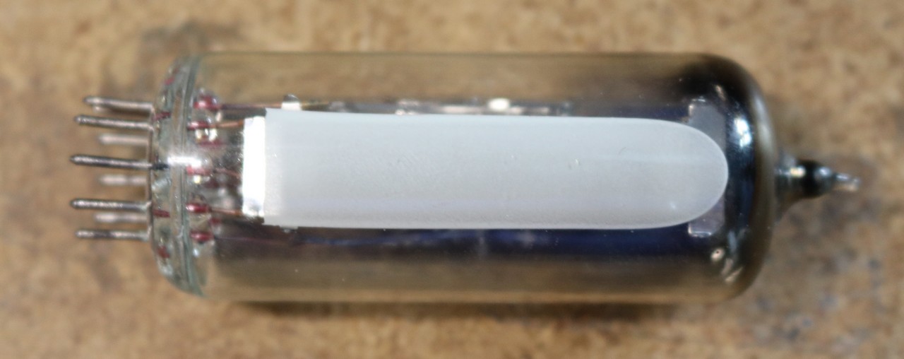
Let’s start with some basics on Magic Eye Tubes. Magic Eye Tubes are vacuum tubes, and you’ll find that they usually (if not always) require a high voltage to drive them. In my case, I’m using EM87 tubes, also known as 6E2, which work best with a 250V supply. These tubes are very plentiful and cheap on eBay. So you’ll need to break out your high voltage supply to start to work on these projects. Please be careful and use appropriate caution around high voltage. The voltages used by these tubes can be dangerous.

EM87 (aka 6E2) Magic Eye Tube

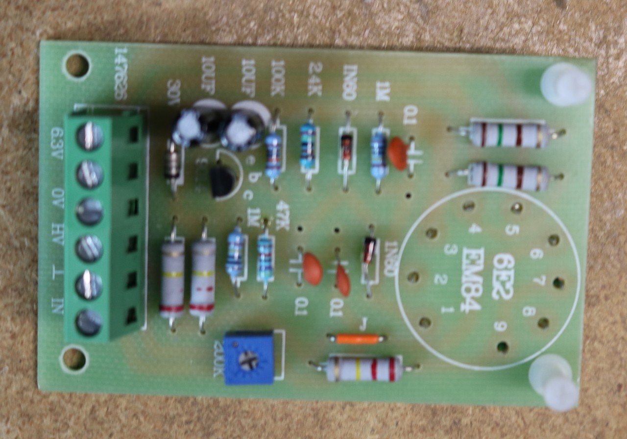
While I already knew enough about the tubes to construct my own driver, I saw that there were some kits on eBay that cost little more than the tube itself, and include the socket and some electronics. So I bought myself three of these kits. These kits implement a simple audio vu meter functionality. They don’t come with a high-voltage supply, so you’ll have to bring your own. Here’s what it looks like unassembled:

The kit came in a baggie

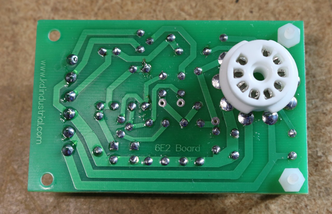
and here’s what it looks like assembled:

Assembled eBay kit, top view

Assembled eBay kit, bottom view

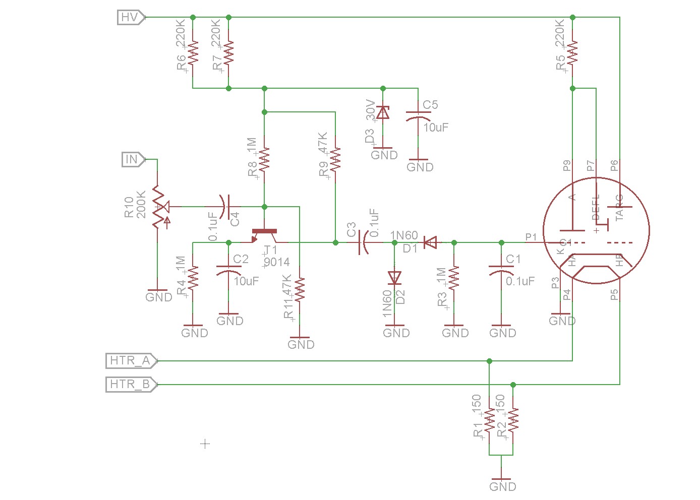
I reverse engineered the eBay board and derived a schematic from it:

Magic Eye Kit from eBay, schematic

Replacing the driver with an Op-Amp

I had some projects in mind, and I knew that I wanted to be able to drive the tube with positive low-voltage signals, for example from a microprocessor-controlled digital to analog converter. I also knew (from reading as well as from experimentation) that I would need to supply a negative voltage signal, from 0 to -15 volts, to control the magic eye tube. This is a perfect opportunity for an inverting op-amp circuit. I’m not going to go into detail to cover op-amps here — I recommend one of Dave’s excellent tutorials at eevblog for that.

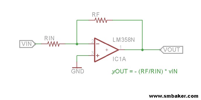
The key thing about an op-amp is that it always tries to make both of its inputs the same and it will adjust its output to accomplish that. It’ll drive its output up or down, all the way to the rails if necessary. This leads to the our basic inverting op-amp schematic and formula:

Inverting Op-Amp schematic and formula

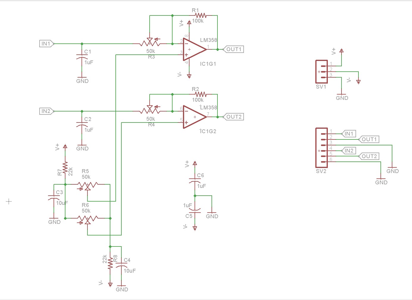
All we have to do is to compute the right value for RF and RIN, and we could turn a 0-2V control signal into 0 to negative 15 volts. Since you get two op-amps per LM358, I put together a basic op-amp driver board:

Inverting Op-Amp Driver Board Schematic

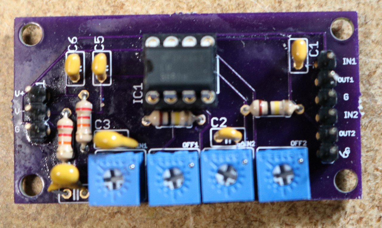
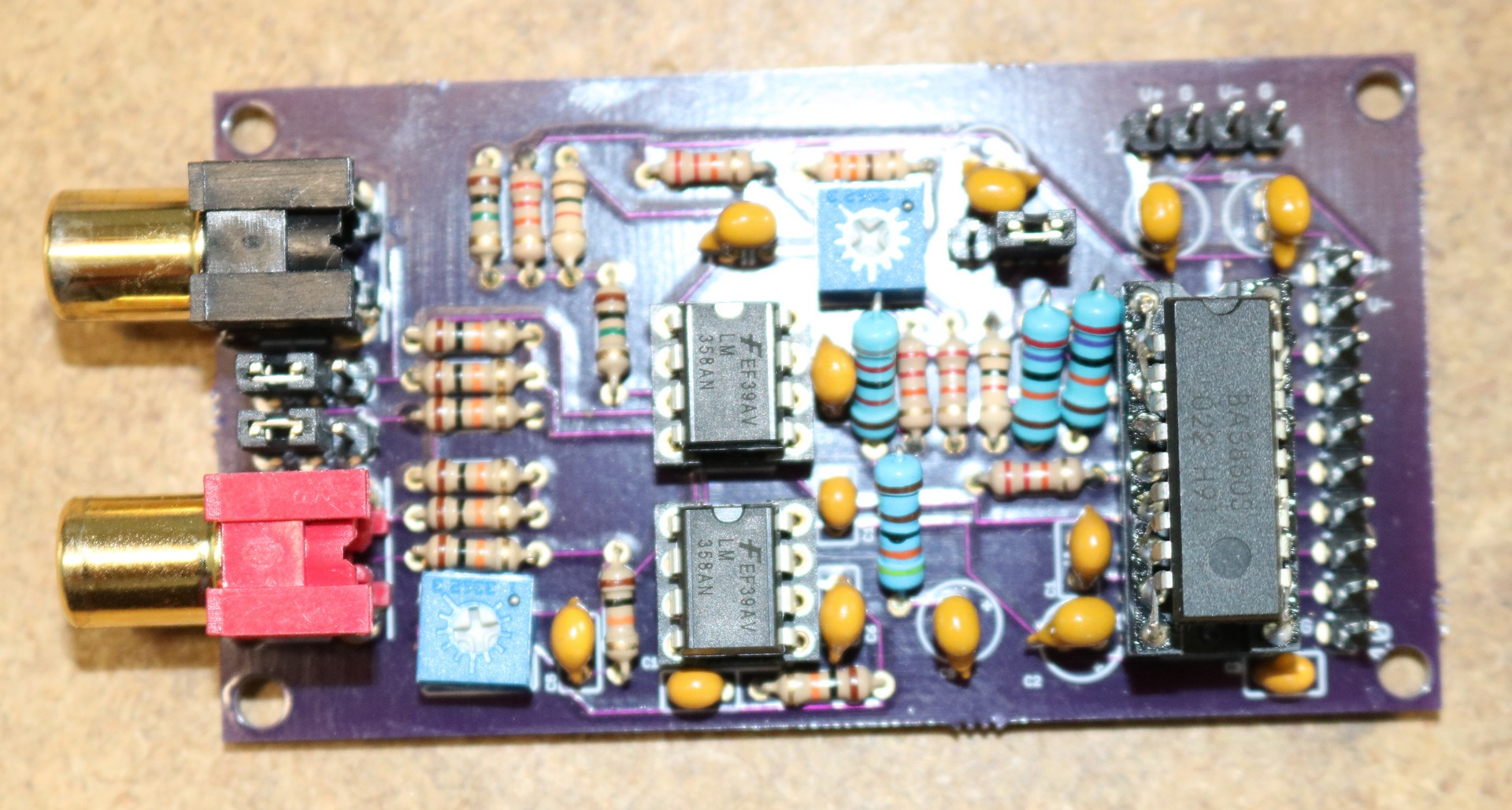
This is an extension of the basic inverting op-amp circuit. Instead of a fixed RIN, a potentiometer has been added. Instead of a fixed value to the + input of the op-amp, a variable source has been provided to control offset (remember, the op-amp will always try to make its two inputs equal, so if we offset one of the inputs, then it’ll offset the output). I have to credit Mr. Nixie at nixiekits.eu for his Magilyzer project, which was very handy to me in selecting the component values for this op-amp board. My completed board is shown below:

Inverting Op-amp driver, completed pcboard

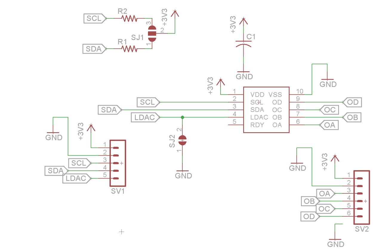
The next step to controlling this with a raspberry pi was to add a digital to analog converter. Fortunately, I had some breakout boards leftover from a previous project:

MCP4728 breakout board, schematic

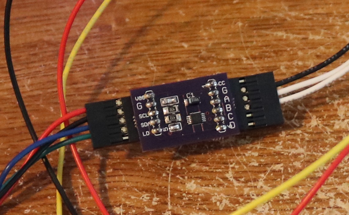
The completed board:

MCP4728 breakout board, assembled

Wiring this up to the raspberry pi is very simple — the SCL and SDA pins connect to the raspberry pi’s SCL and SDA pins (I2C interface). The Vcc and GND connect to the raspberry pi’s +5V and ground. The MCP4728 provides four outputs. We only need one of them to drive the op-amp board and control our magic eye tube.

Magic Eye Tube PC Monitor

$
0
0

This is my third video in a series on magic eye tube projects. For background, please view the earlier blog post on magic eye tubes first.

Overview

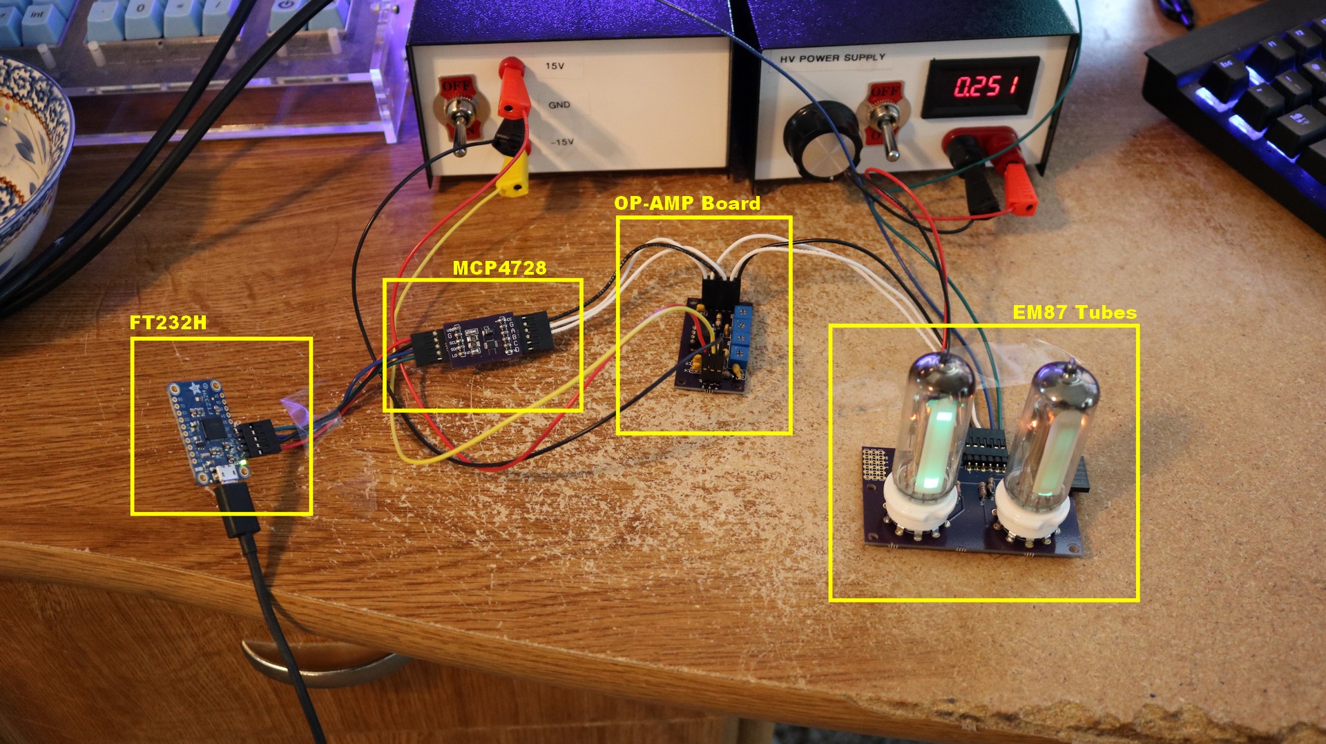
The idea behind this particular project is to control the magic tubes from a Windows PC and display information about the PC. I figured it would be interesting to show two metrics — CPU performance and network performance. To do this, we’re going to use two magic eye tubes, an opamp board, an MCP8728 DAC, and a FT232H breakout board. Here’s an overview diagram:

Magic Eye Tube PC Monitor Diagram

The first part of the pipeline is the FT232H breakout board. I obtained this from Adafruit. The FT232H is a pretty versatile board, it can do serial communication, I2C communication, SPI, and even GPIO. I’m going to be using it as a simple USB-to-I2C adapter. The Windows PC can send commands over USB to the board, and the board will convert those commands to I2C and send them to the next unit in the chain, the MCP4728.

The MCP4728 is next up in the pipeline. It takes the I2C digital control from the FT232H and converts it to an analog signal. The MAC4728 is a 12-bit DAC converter, giving us 4096 levels of output. It supports four channels (we only need two, one for each tube). There’s a built in internal 2V voltage reference. So what this gives us is the ability to output a pair of 0-2V signals with 4096 bits of precision. We only use two of the outputs (“A” and “B”) and we send them to the next unit in the chain, the op-amp board.

The op-amp board is described in my previous magic eye tube article, so I won’t say much about it here. To control the magic eye tubes, we need a signal that varies from zero to minux 16 volts DC. We will use an inverting op-amp circuit to take our 0-2V control signal (from the MCP4728) and convert it to the 0 to -16V output signal. I use a dual opamp chip, the LM358N, so we can handle both channels from the same board. Each channel includes both an offset and a gain potentiometer.

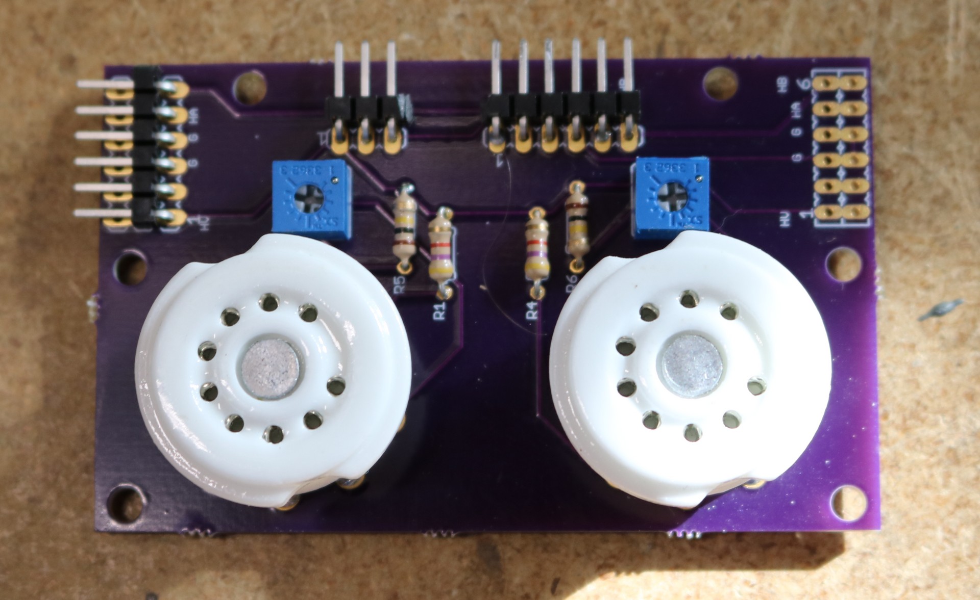
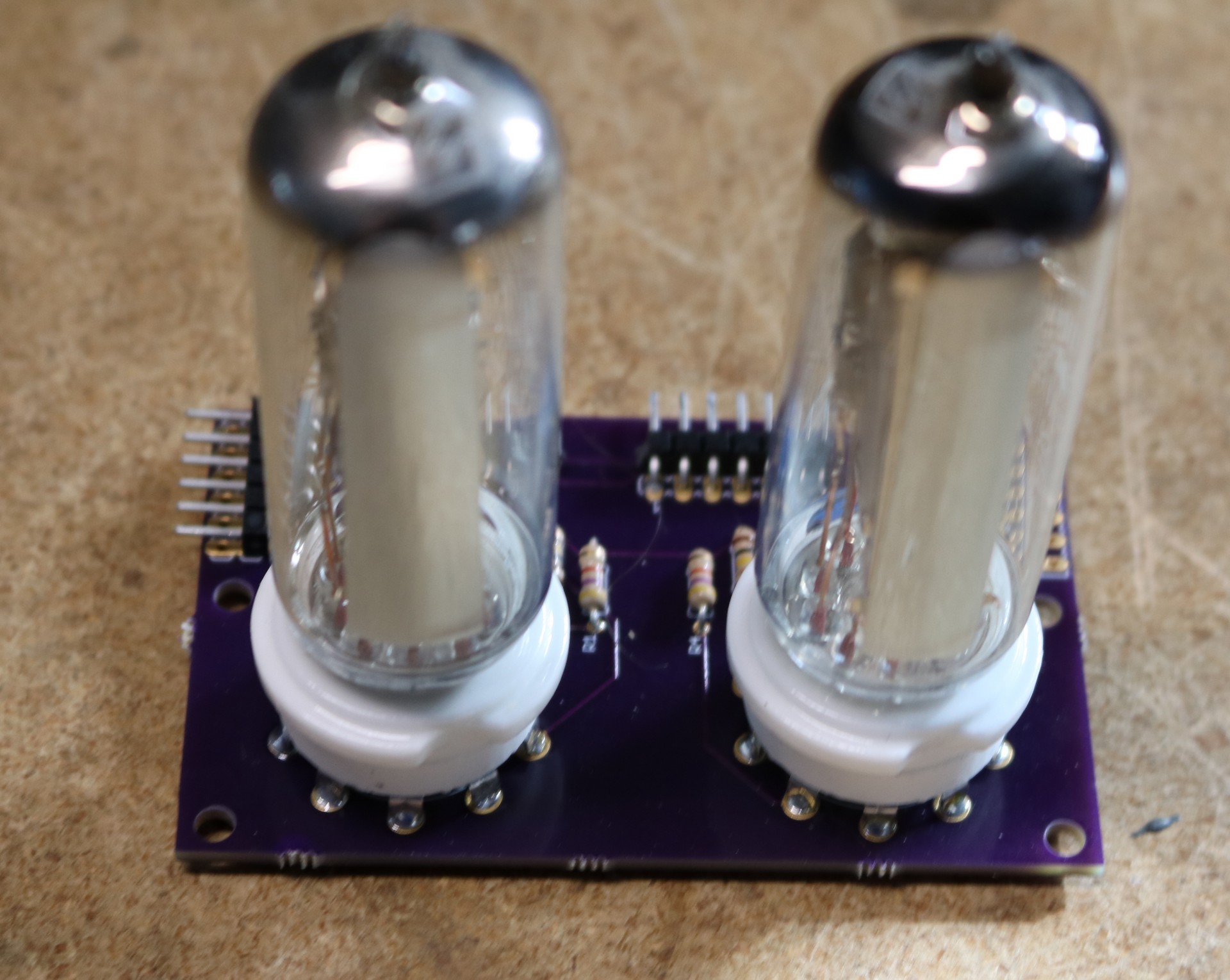
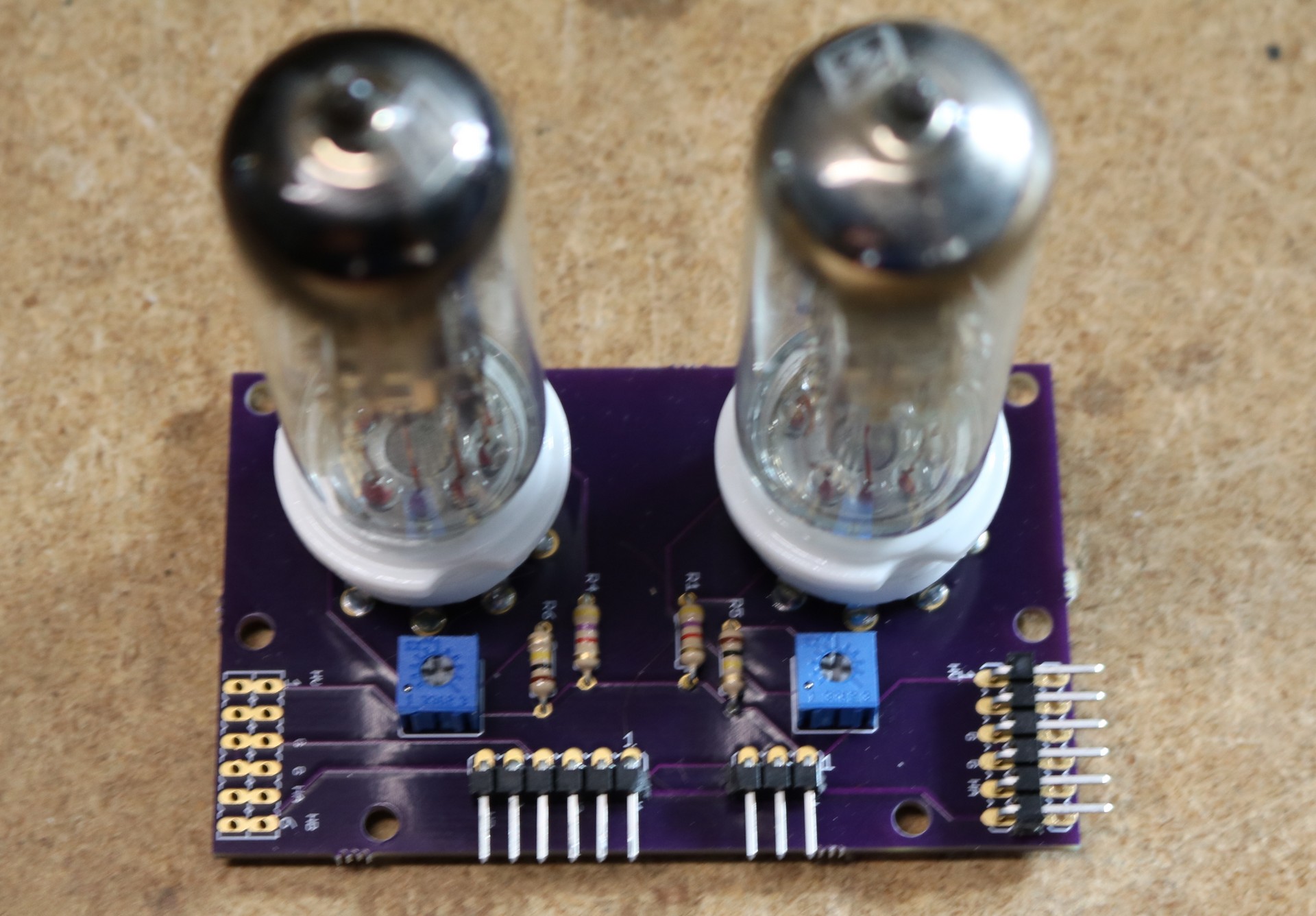
Finally, we get to the magic eye tubes themselves. I’m using EM87 tubes on a custom breakout board that I had fabbed at osh park.

EM87 breakout board

EM87 breakout board with tubes installed

Proof of concept:

Below is a picture of the whole setup sitting on my desk:

Magic Eye Tube PC Monitor, Assembled

Source Code

You can find the windows source code in my github repo at https://github.com/sbelectronics/pc-mageye-mon

Magic Eye Tube Audio Spectrum Analyzer

$
0
0

This is the fourth and final in my series of magic eye tube projects (well, unless I can find something else interesting to do with them!)

For background, please see my first magic eye tube post.

This project was heavily influenced by Mr Nixie’s Magilyzer project, which you can find here.

If you recall from the previous video, I had designed some two-tube magic eye tube modules, here’s a picture:

Dual Magic Eye Tube Module, First Prototype

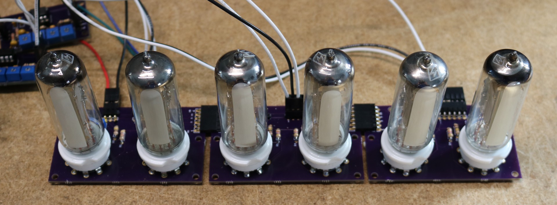
My plan was to be able to string them together into a string of six modules as so, and then connect them to the op-amp boards that I had demoed in my previous video, like so:

Magic eye tube modules, chained together

I then built a spectrum driver board, that uses the BA3830S chip. It was based heavily on the design of Mr Nixie’s design. Here’s a picture of the spectrum analyzer board:

Spectrum analyzer driver board

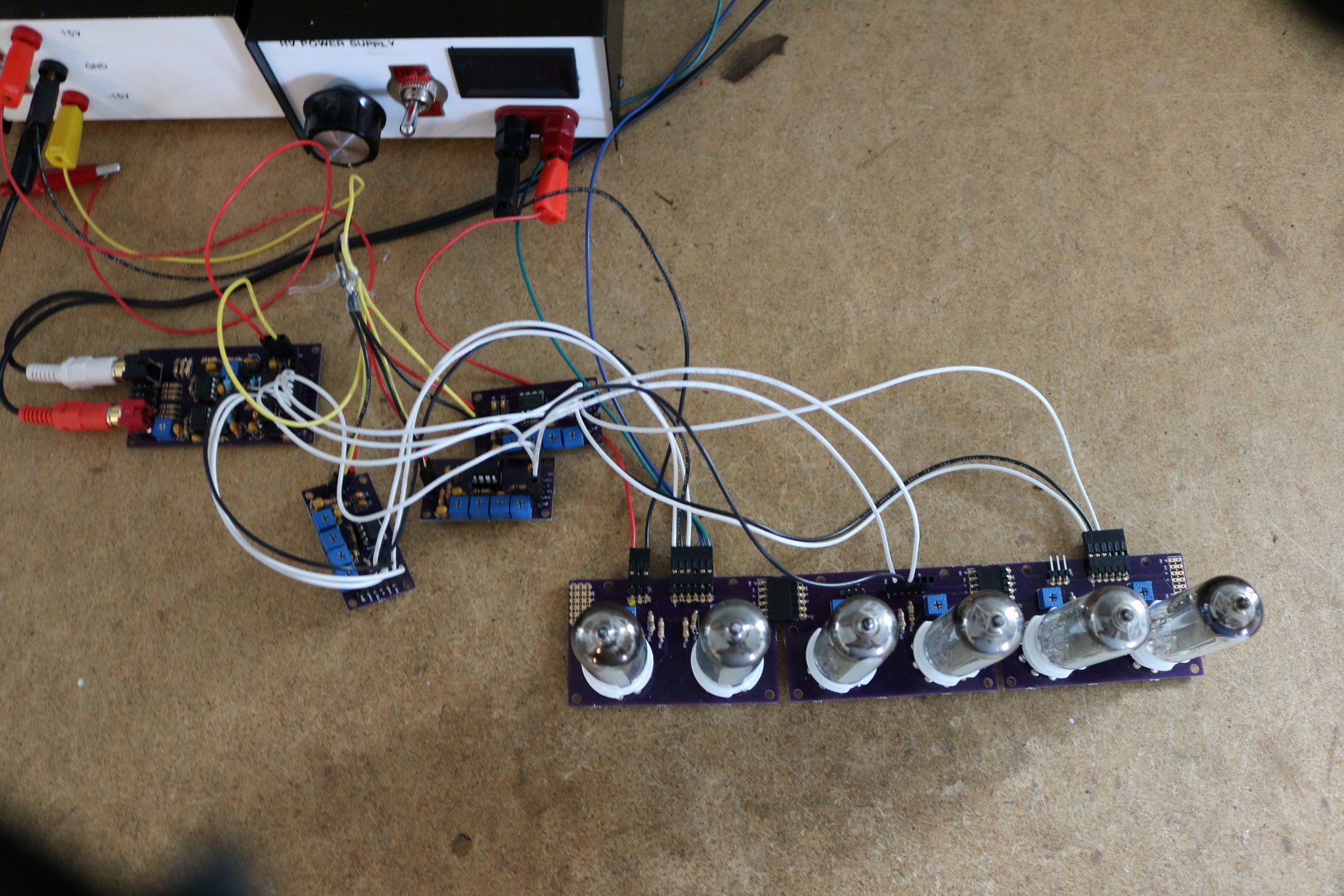
Putting it all together we have a functional spectrum analyzer, albeit somewhat of a ratsnest of wires and boards:

Magic eye tube spectrum analyzer prototype

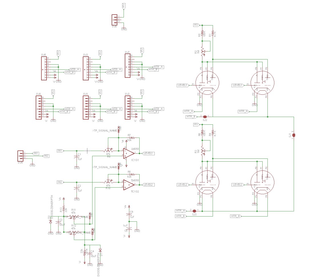
Along the way, I decided it was really cumbersome to have to deal with the op-amp boards and the wiring between the op-amp boards and the magic eye tube boards, so I redesigned the magic eye tube boards to include the op-amps. This minimizes the amount of wires and boards involved in my first prototype. Here’s the schematic of the revised dual magic eye tube board:

Schematic for dual magic eye tube board, revised version

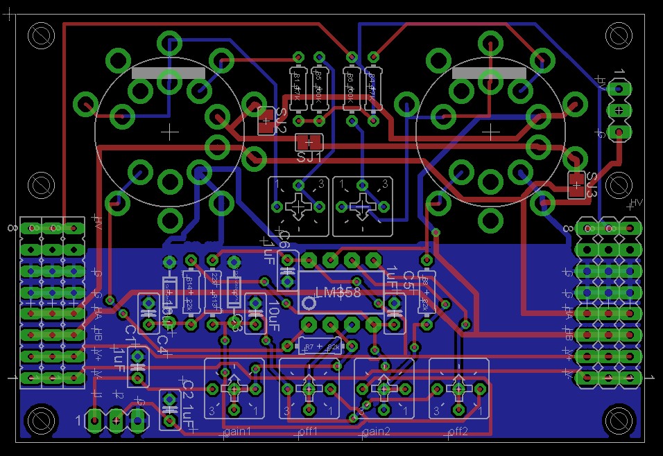
Apparently, I forgot to take out the camera that weekend, as I never took a picture of the new modules. I can show a photo of the board layout though:

Dual magic eye tube board, revised layout

The schematic may confuse some folks why it looks like there’s two sets of magic eye tubes. The reason is because I put two footprints for each tube on the board. One footprint fits the nice ceramic magic eye tubes that you can buy on ebay. The other footprint fits pin sockets (Typically called “Mouser Pins”) that you can buy from Mouser. My original plan was to use the Mouser Pins, but it turned out that the ceramic sockets are really convenient. As you can see in the above board, there’s room for the opamp, the gain and offset controls, etc. Each board is designed so that it can be daisy chained to the next, and there’s a three pin header that allows you to control the tubes (one signal pin per tube, plus a ground)

After this, I designed yet another layout for my high voltage power supply that matched the size of the driver boards. Then I stuffed it all in to an acrylic case.

[TODO: Add Picture of the Completed Project]

Product Reviews: Mooshimeter, Raspberry Pi Black Slices Case, Powerhorse Surface Cleaner

$
0
0

Here are a trio of product reviews. The first is the Mooshimeter:

Mooshimeter is a DMM accessory for use with your iPhone, iPad, or Android device. It communicates over bluetooth to the device. It supports multiple channels so you can measure both current and voltage simultaneously (very handy!). I needed a secondary DMM for the bench, and it seemed like a good buy. I’m very pleased with it and have used it for several projects already. I highly recommend it if you need an additional DMM. It can graph measurements over time which is great for seeing trends.

Next up is the Raspberry Pi Black Slices Case:

I needed some cheap cases for some raspberry pi projects. Often I make my own cases using Ponoko, but for something simple, it was easy just to find a cheap one. When looking for the black slices case, make sure to price shop. I found mine for ~ $4.25 each on eBay, plus approximately $2 shipping. On Amazon they are selling for as much as $19.95. It’s a cheap case but seems reasonably durable and easy to put together. I like that I can leave the top cover off for projects that need an exposed top.

Finally we have the Powerhorse Surface Cleaner

What? This isn’t an electronics project or tool!?!? Oh well. It gets lumped into this week’s review page. I needed to power wash the front and back patios of my house. I tried it with the nozzle that came with my pressure washer and it just wasn’t good enough. So, I bought this surface cleaner from Northern Tool. I’d say it cleans at least 5 times faster than the nozzle that came with my power washer, and does a far more thorough job.

Building the Dutchtronix Scope Clock

$
0
0

I was browsing the forums one day at EEVBLOG (where they like to talk about oscilloscopes and DMMs all day long, every day) and I saw mention of the Dutchtronix scope clock. Deep down I knew it and scope clocks like it existed, but I’d never taken the time to order one, until now.

So what is a scope clock? It’s a small PCB with a microcontroller that outputs the appropriate X and Y signals to turn your oscilloscope into an analog or digital clock. Why would you need such a thing? It’s purely a frill, since it’s going to tie up a perfectly good oscilloscope. I suppose you could build your own clock using a CRT, high voltage supply, and some drivers. I’m planning on doing that at some point whenever I get the spare time to learn whatever I need to do to get my own CRT up and running.

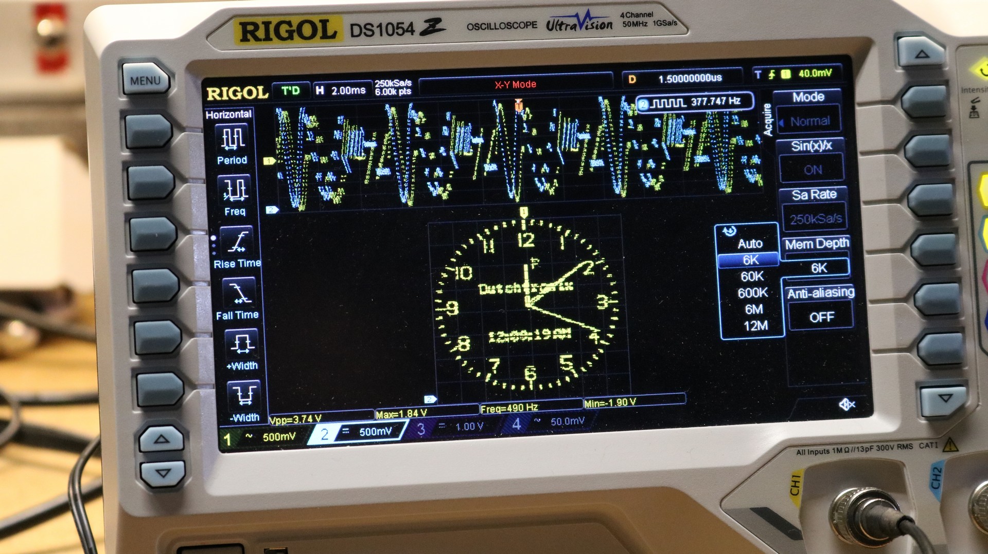
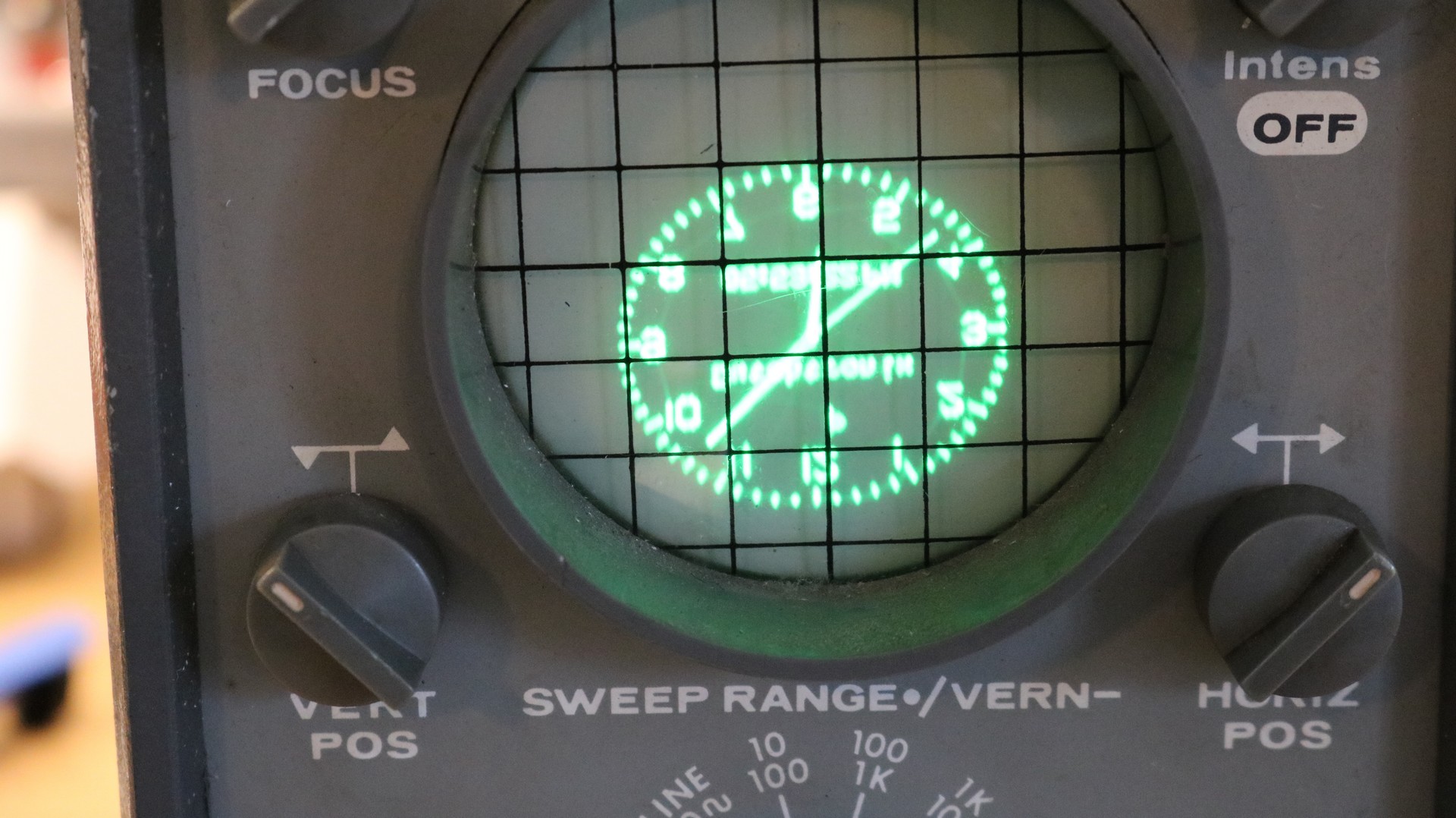
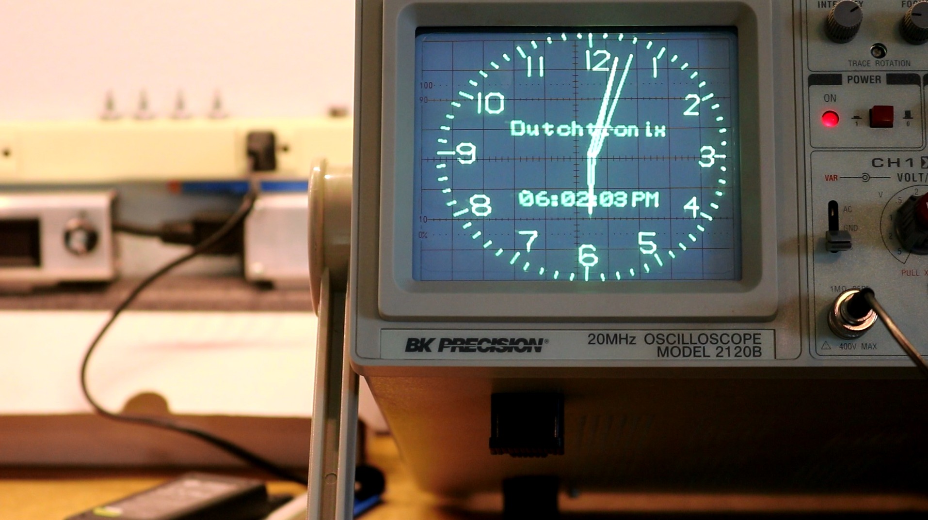
I did try out the scope clock on three of my oscilloscopes:

Scope Clock on DS1054Z

Scope Clock on Eico 430

Scope Block on BK Precision 2120B

In my opinion the BK Precision Analog Scope is the best of the lot, producing the clearest image. My newest scope, the Rigol DS!054Z suffers from a grainy picture because of the way it does XY mode — it’s not a true XY mode, it’s really just sampling both channels in YT mode and then computing the XY data from it. You also can’t go full screen XY mode with the Rigol. The Eico 430, a very old scope filled with vacuum tubes has no invert control and doesn’t even have a DC mode. It’s always operating in AC mode, and that causes some variation in the up/down position of the display, leading to a fuzzy image on camera.


Intro to Z80 Retrocomputing

$
0
0

I’m going to do a series of blog posts on retrocomputing.

In this first video, I introduce the retrocomputing platform that I’m going to be using. It’s the RC2104, by Spencer, who goes by the handle Semachthemonkey on Tindie. I purchased one of his RC2104 “full monty” kits and assembled and tried it out in the video above.

Introduction

So why did I choose the RC2014 and the Z80 microprocessor for my retrocomputing projects? First, I’ve never owned a Z80, so it was an opportunity for something new. Second, I liked the design of the RC2104 backplane. It offers plenty of room for expansion, for me to design and integrate my own modules. 40-pin headers are easy to come by and easy to work with. Once you populate the backplane out with a bunch of boards for various peripherals, it makes an impressive collection of PC boards and chips.

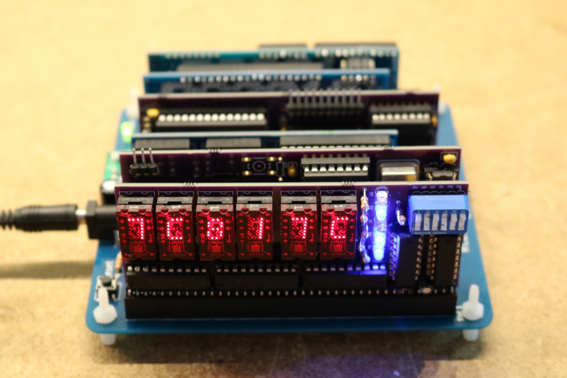
rc2014 with some additional boards

A basic RC2014 build consists of: CPU, RAM, ROM, Clock, and Serial. That’s a total of five boards on the backplane leaving room for three additional boards. In the picture above, I’ve added a bus monitoring board, a real-time clock board, and replaced the default Clock board with an I2C bus supervisor that I’m still working on. I’ll be describing the various add-on boards in subsequent blog posts.

Architecture

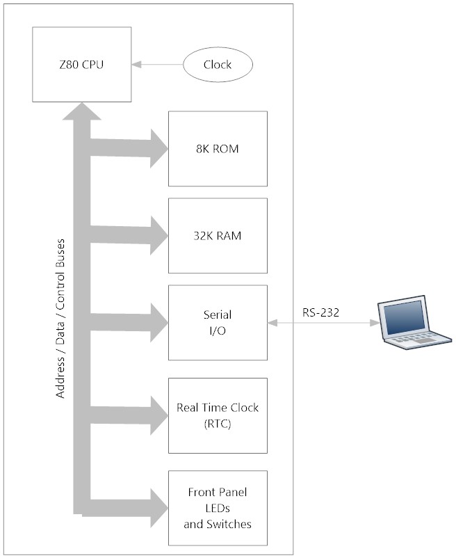
Retrocomputer Architecture

The Z80 has an Address, Data, and a control bus. The Address bus is 16 bits consisting of address pins A0-A15. The Data bus is 8 bits consisting of D0-D8. The Control bus has a number of signals, the most important ones to us when interfacing to peripherals are M1, WR, RD, IORQ, and MEMRQ.

Modules

The RC2014 Full Monty kit provided me with the standard set of modules that I needed to get the computer working. They are:

  • CPU – The Z80
  • ROM – 27C512 64 KB ROM, selectable in 8KB banks. This allows you to theoretically have 8 different ROMs available to boot, selectable by jumper.
  • RAM – 62256 32 KB RAM
  • Clock – 7.3728 Mhz crystal that drives a 74HC04 hex inverter. This clock drives both the Z80 and the UART on the serial board.
  • Serial I/O – MC68B50 UART. It’s broken out to a header than can be directly connected to a FTDI cable, or you can populate the MAX232 socket for a real 9-pin serial port.

Along with the basic kit, I also purchased the Digital IO module. This consists of 8 buttons and 8 LEDs, and gives the first time retrocomputer builder something that “feels” retro.

Even before I received the kit, I had also started designing my own modules. The ones that I have built and/or am in the process include:

  • Real Time Clock (RTC) and digital output – these will allow me to create a basic Nixie Tube Clock
  • Bus Supervisor – By connecting some I2C I/O expanders to the bus, I hope to be able to put the Z80 into wait mode and takeover the bus using a raspberry pi. The idea is to be able to use the bus supervisor for assembly language development. I could in theory replace the ROM with another RAM chip, load programs into the RAM using the bus supervisor, and have a very rapid development cycle.
  • Bus Monitor – Using some LED displays, I can show the values on the address and data buses.
  • Single Stepper / Slow Stepper – Once I build the Bus Monitor, I realized the Z80 runs a little too fast for the Bus Monitor to be interesting. Slowing the Z80 down and single-stepping it will make the Bus Monitor a little more interesting.
  • Speech Synthesizer -  The retrocomputer needs a 1980s style voice.

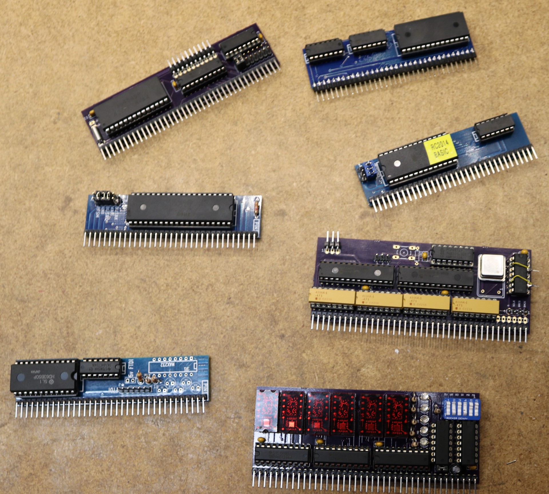
Some of these modules I’ve built already. Some I’m still developing. I’ll be placing links to the associated blog pages as things come along. Below is a picture of a pile of modules, some from the Full Monty kit, some that I built myself:

Modules for RC2014 (clockwise from bottom left: Serial, CPU, RTC, RAM, ROM, Supervisor, Monitor)

Interfacing Basics

I started this with zero knowledge of the Z80, and managed to piece together some interfacing basics by looking at the work over others. Some notable and very useful websites are http://rc2014.co.uk/ and https://z80project.wordpress.com/.

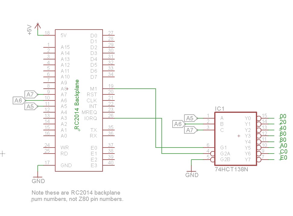
Interfacing a peripheral device generally means adding it to the Z80’s IO space. To do this there are four signals of interest to us: M1, IORQ, RD, and WR. The M1 signal is active low when the Z80 is fetching an instruction from memory or when it’s acknowledging an interrupt. IORQ is active low when an IO operating is being performed. RD and WR are active low if the operation is a read or a write, respectively. This allows us to use a 74HCT138N as a basic IO address decoder:

IO address decoder using 74HCT138N

The upper three bits are used to select the IO addresses 00, 20, 40, 60, 80, A0, C0, or E0. That allows us to place a peripheral at any of 8 possible IO address spaces. In the above example, I didn’t do anything with the RD or WR pins. If you wanted to, you could connect RD or WR to the 74HCT138N’s G2B input, and this would cause the IO address decoder to only select the attached peripheral for reads or writes. The output of the 74HCT138N typically goes to the chip select device of the chip you’re attempting to interface to. It’s this basic IO decoder that I will  end up using in most of my peripheral boards.

There are some important addresses that you should avoid, because the RC2014’s default boards use those addresses. The Serial IO board occupies addresses 80 to BF. The RC2014 Digital IO board by default occupies addresses 00 though 7F.

Logic Families

I’ve often not put a whole lot of thought into logic families — to me, if something calls for a 74xx04, I’ll use a 74LS04 just as quickly as I’ll use a 74HCT04. This Z80 retrocomputer build is the first time I’ve experienced a project where it really matters. Different logic families will place a different load demands on the Z80 microprocessor, which can only supply a few milliamps of drive to its pins. You can quickly load a Z80 down with LS parts. For my boards, I’ve been trying to exclusively use HCT parts. HCT are low power devices that still support TTL level voltages for high and low states.

You might run into a few of my blog posts or schematics where I’ve referred to a part as an HC or an LS. If so, that’s probably a mistake and I really meant to say HCT. If I do specifically choose a part that’s not an HCT then I’ll try to explain why.

Power

The RC2014 backplane can be powered by 5V, or you can add a 7805 regulator so that you can power the backplane from other voltages. I really like powering my projects from 12V, so I added a 7805.

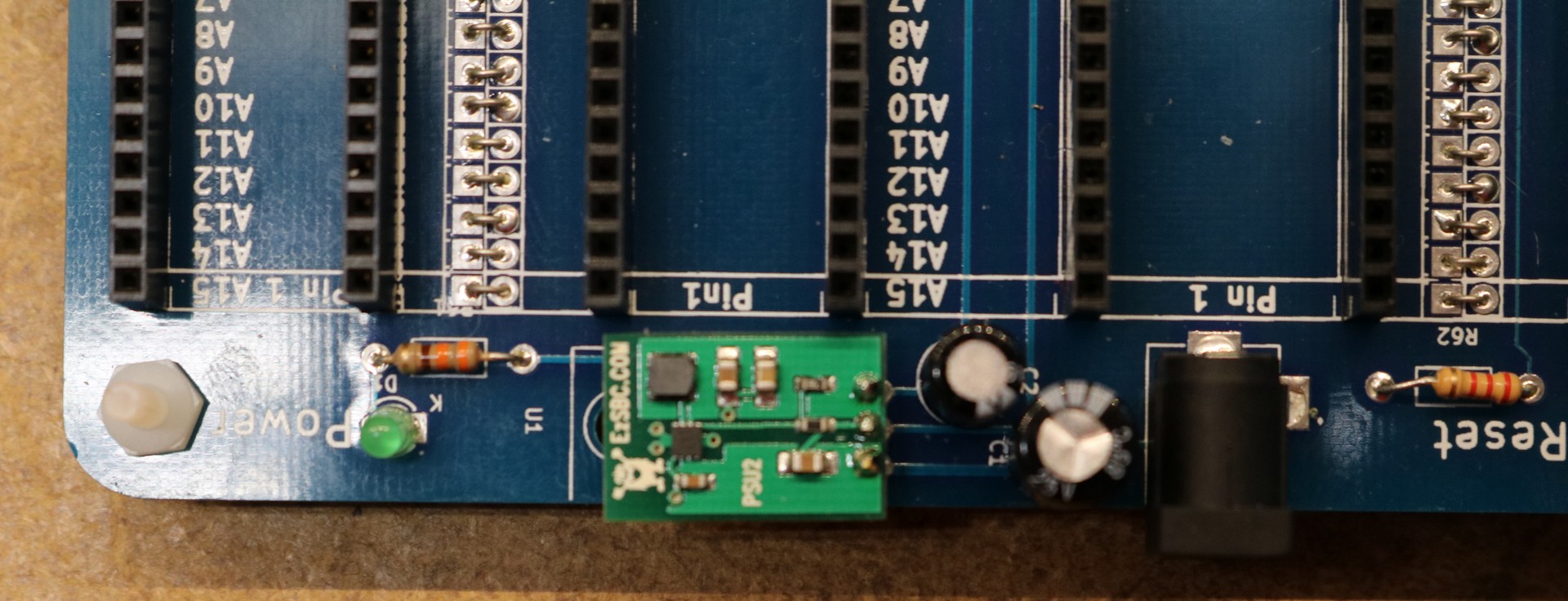
This worked pretty well until I added one of my boards that had a whole lot of LED displays, and I overloaded the 7805 regulator and it went into thermal shutdown. It burned my finger too, when I touched it. I ended up replacing the 7805 with a switching regulator made by EZSBC. These little EZSBC regulator boards are pin compatible with the 7805, more-or-less about the same form factor, and use a switching regulator. Yes, it feels like cheating to have a modern surface-mount switching regulator in my retrocomputer project, but it also eliminated burnt fingers and thermal shutdowns. Here’s a picture of the switching module mounted in place of the 7805:

Switching power supply in place of 7805

Programming in BASIC

Basic was the first programming language I ever learned. It’s been a long time, but it came back to me.

I believe the particular implementation BASIC language used by the RC2014 is (either outright or derived from) this one by Grant Searle. If you’ve ever programmed any form of BASIC, then this should seem pretty familiar to you. It is handy to look over Grant Searle’s list of included keywords to know what the BASIC implementation does and does not support. While writing my simple programs, I often found myself trying to use keywords that weren’t implemented.

I found the easiest way to load and save programs is to write them up in my favorite text editor on my windows PC and “paste” them into the terminal program connected to the RC2014’s serial port. Beware that pasting a long program at 115200 baud can send data faster than the retrocomputer can keep up with it. I found it helpful to add a 35 millisecond line delay in my terminal program. The terminal program I use is SecureCRT by VanDyke technologies. It’s my go-to program for SSH, and I was happy to find that it will also talk to serial devices.

Scott’s github repo

My github repo containing various bits of source code and other useful things for the boards I’m working on is located at https://github.com/sbelectronics/rc2014. For example, it contains the BASIC program source for my RTC board and Nixie Tube clock.
Z80 Retrocomputing 2 – Real Time Clock for the RC2014

$
0
0

In this post, I create a Real Time Clock (RTC) board for the RC2014

This is the second in my series of Z80 retrocomputer blog posts. If you haven’t already done so, then it might be helpful to start at the first post.

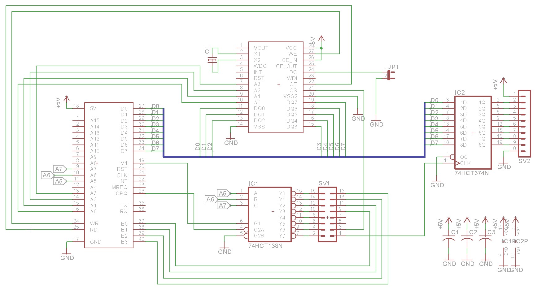
I wanted my first application of the Retrocomputer to be a Nixie Tube Clock. In order to do that, we have to make the retrocomputer tell time. There are a lot of real-time clock chips out there. Modern devices will usually be I2C or SPI. For something more compatible with the Retrocomputer, I went with the BQ4845. I got the idea of using the BQ4845 from a number of sites, most notably Nathan Dumont’s blog post.

Here’s a schematic of the board that I developed:

Z80 real time clock (RTC) using BQ4845

Let’s start with the address decoding. This was already described in my first retrocomputing blog post, but it’s worth describing again here. The 74HCT138N is a 3-to-8 decoder. We will use it to take 3 of the Z80’s address pins (A5, A6, A7) and generate one of eight outputs based on those pins. This will map to IO addresses 00, 20, 40, 60, 80, A0, C0, or E0. By default I attached the RTC to C0 as this avoids both the RC2014 serial board (80-Bf) and the RC2014 digital IO board (everything below 80).

The 74HCT128N is also connected to the M1 and IORQ pins so that it will only be enabled when M1 is high and IOREQ is low. This ensures that we’re enabling on io reads and writes and not some other kind of operation.

The Z80’s RD and WR pins are connected to the BQ4845’s OE and WE pins. That makes sure the BQ4845 writes when the Z80 wants to write and reads when the Z80 wants to read. Address pins A0 to A3 are connected from the BQ4845 to the Z80, allowing the Z80 to select any of the 16 registers that the BQ4845 supports.

I also added an output driver to the board, a 74HCT374N. I knew that I wanted to be able to drive some of my nixie tube displays, and there was spare real estate on the clock board, so it seemed a logical place to add an output driver. The 74HCT374N is by default connected to Y7 on the 74HCT138N, placing it at IO port E0.

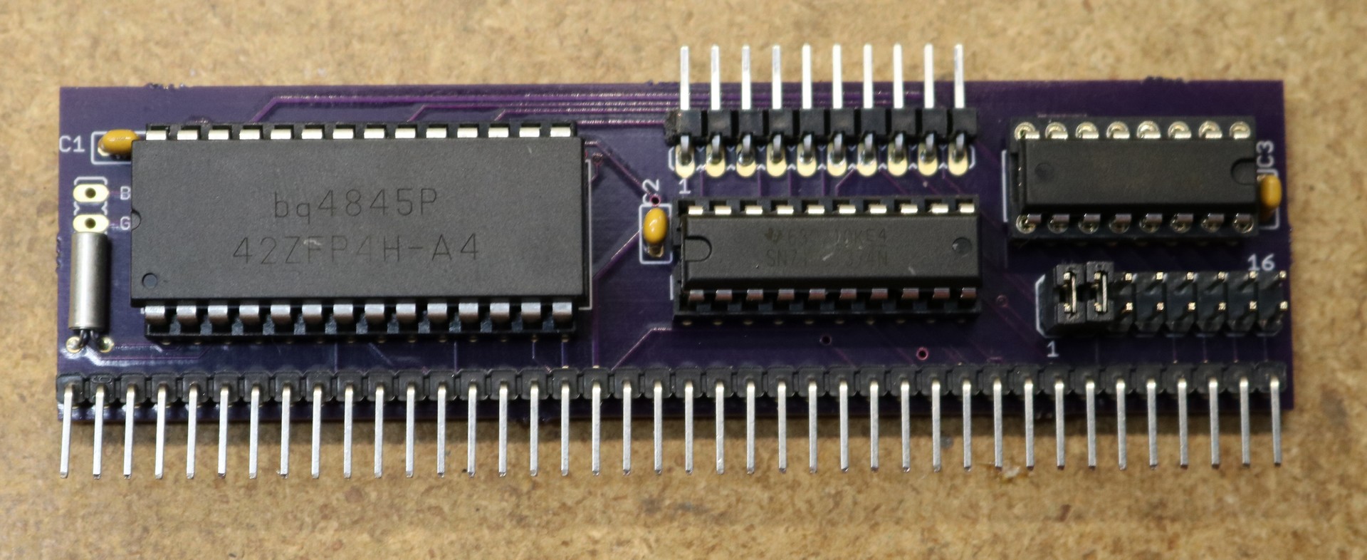
JP1 is a 2-pin jumper that allows you to attach a battery backup to the real-time clock should you wish to do so. Here’s an image of the assembled module:

Z80 RTC board, assembled

Next up are the IN12 Nixie Tube display boards:

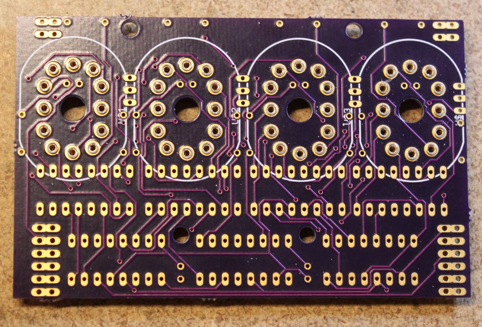
IN12 Nixie Tube Display Boards

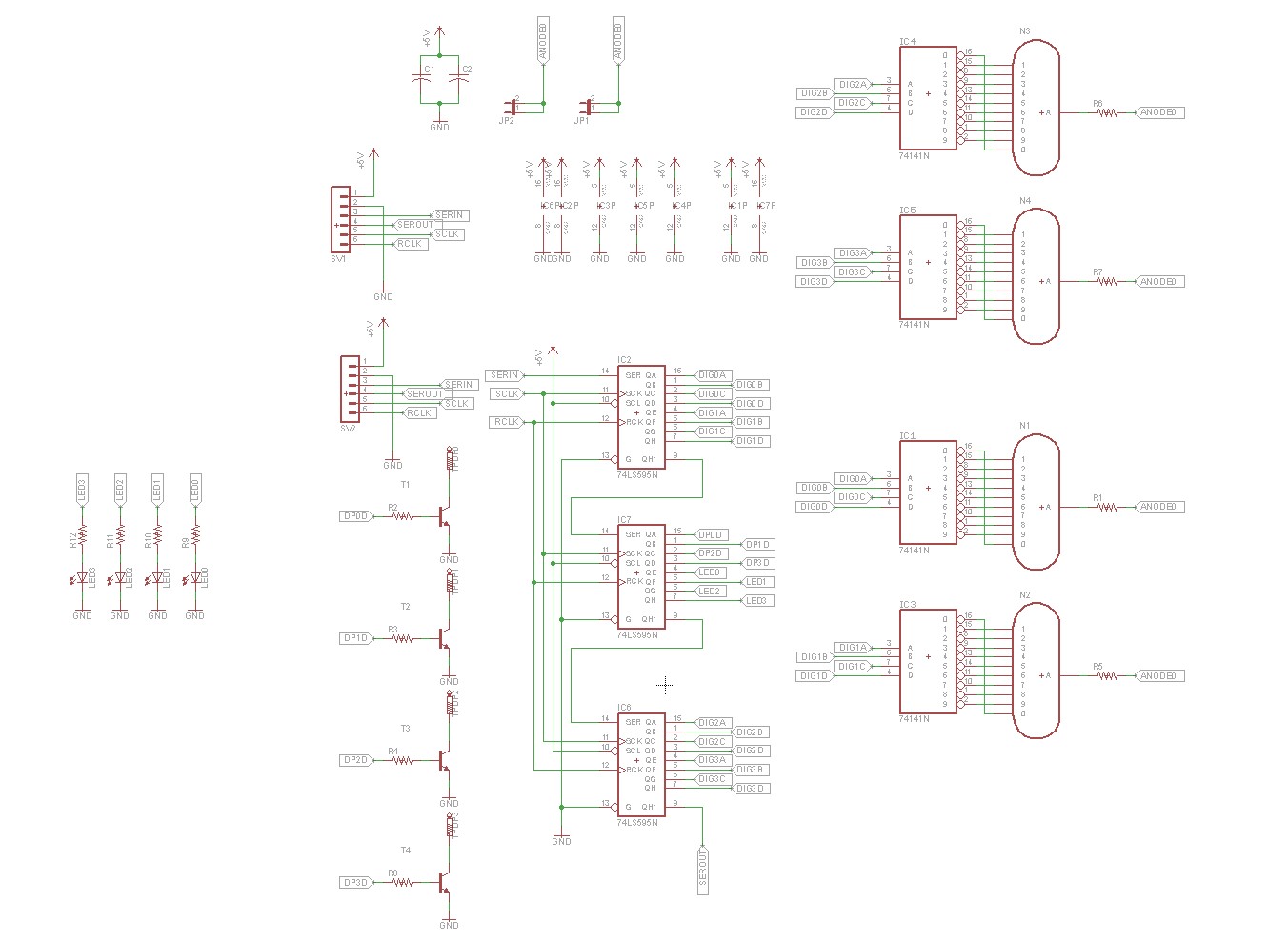
These are leftover boards from my Nixie Tube Calculator project. My final boards used I2c, but my first set of boards used 74LS595N shift registers, and shift registers are perfect way to interface to a retrocomputer like the RC2014. Each Nixie Tube Display board uses 3 shift registers for a total of 24 bits of output. I use two display boards, for a grand total of 48 output bits. Here’s a picture of the board, with mouser pins installed for the tubes, before I added the ICs:

Nixie Tube PCB

To interface these boards to the retrocomputer, I wire the 74LS595’s SERIN, SCK, and RCK pins to the 1Q, 2Q, and 3Q outputs on the 74LS374N on the clock board. This allows us to bit bang out all 48 bits necessary to the display boards. We can do this fast enough, even from a program written in Z80 basic.

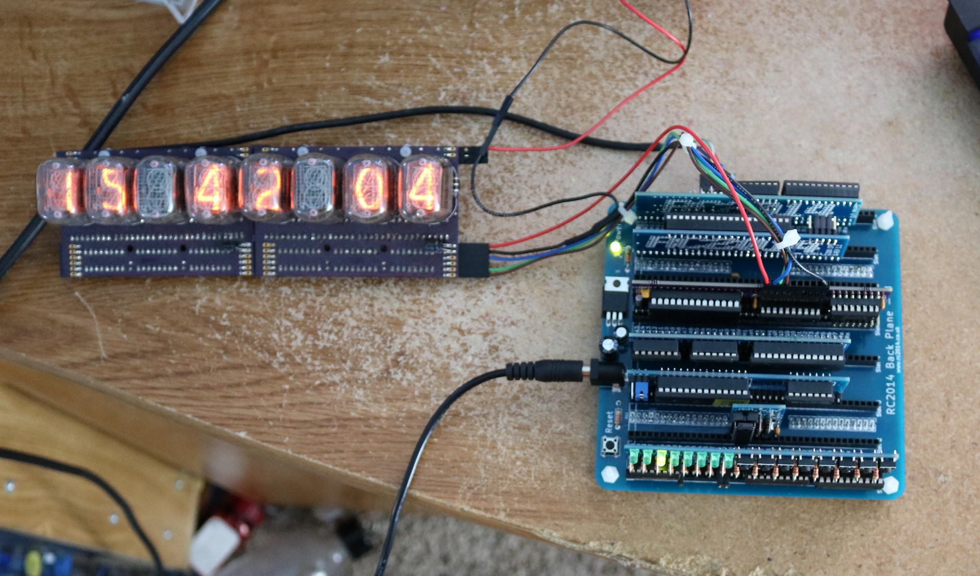
Here’s a picture of the whole thing wired together:

RC2014 with RTC board and Nixie Tubes

Source Code

The source code for the nixie clock is available in my github repo at https://github.com/sbelectronics/rc2014.

Z80 Retrocomputing 3 – Bus Monitor Board

$
0
0

I wanted more lights on the retrocomputer, so I decided to add a bus monitoring board.

For a brief introduction to my retrocomputing posts, please start at the first one.

So what exactly does the bus monitor board do? It monitors the Z80 address and data buses and displays the current values on those buses on hexadecimal displays. This allows you to, for example, see what IO ports are being read and written, or what memory addresses are being written.

When designing this board, I faced a few options as to how to display the output. A lot of retrocomputer designs will use simple LEDs and display the output in binary. That’s neat (blinking lights are always neat) but not too useful unless you’re quick at doing binary to hex conversion in your head. I looked around on ebay, and eventually came up with some hexadecimal displays, the TIL311. The TIL311 can display a single hex digit (0,1,2,3,4,5,6,7,8,9,A,B,C,D,E,F) from a four-pin binary input. It has an onboard TTL driver to do this.

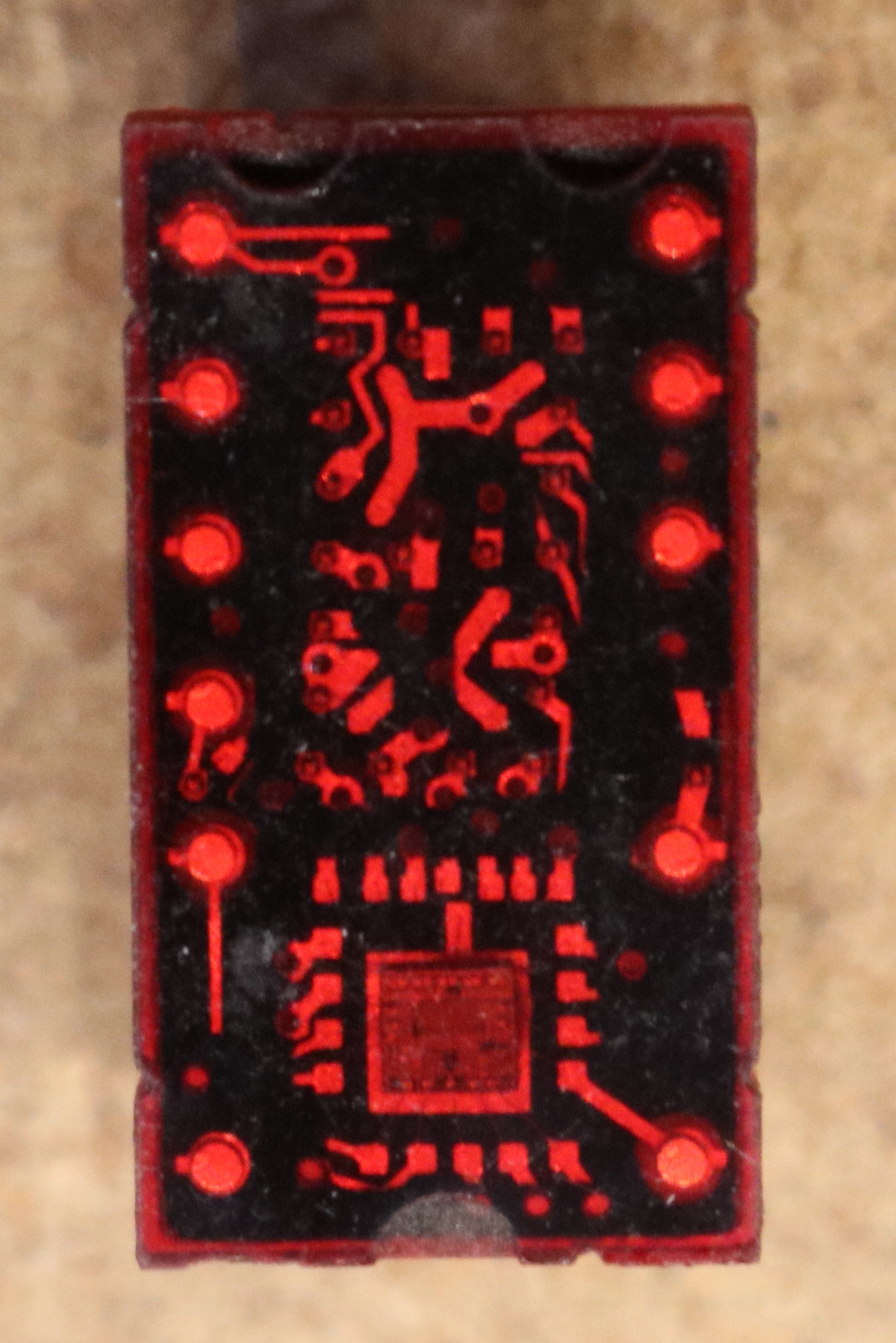
TIL311 hexadecimal display

Above is a picture of one of the TIL311 I purchased on ebay. It’s really very small, the whole thing fits a 16-pin DIP socket. The LEDs are in the top half of the TIL311, and the TTL driver logic is in the bottom half.

Examining the TIL311 datasheet, I came across the first hurdle to be overcome. The TIL311 is a TTL device. It will sink 1.6 ma if a logic low is placed on one of the input devices. The Z80 only provides 1.8 ma of drive current, and the RC2014 is designed with an unbuffered data bus. A single TIL311 display would pretty take the entire Z80 output drive current, severely loading the bus. For this reason, I had to add buffers in front of the TIL311. I chose the 74HCT244N.

The next question was what data I wanted to display on the TIL311. At first this seems obvious, I want to display 16-bits (four hex digits) or address bus and 8-bits (two hex digits) of data bus. However, just attaching the TIL311 to the bus and displaying everything isn’t necessarily a good idea. The RC2014’s Z80 is running at 7.3728Mhz, and simply displaying the bus during normal operation is going to lead to a rapidly changing unreadable display. It’ll change so fast that you probably won’t even be able to see it.

The solution I chose was to add some configurable latching capability. I broke out the M1, MREQ, IOREQ, RD, and WR signals to a dip switch so that those signals can be used to trigger the latch on the TIL311. If you select M1, then in theory you should be able to see every instruction load address. If you select IOREQ then you should be able to see every IO request. Watching instruction loads at 7.3728Mhz is still not something the human eye can perceive, but io requests happen much less frequently and you can actually see stuff happen.

Furthermore, I’m planning on adding a single-stepper and a slow clock board at some point, and once that’s done, then watching memory requests and instruction fetches may be useful.

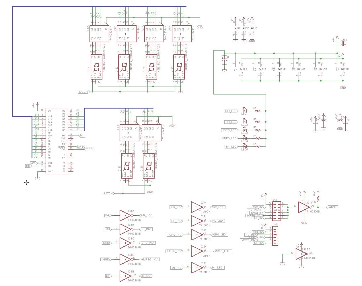
Here’s the resulting schematic of the bus monitor board:

Z80 Bus Monitor Schematic

The TIL311 displays and the 74HCT244N buffers should be pretty straightforward. We can probably use some description of what all of the hex inverters are doing… In addition to buffering the address and data pins, we also need to buffer any control signals we want to display. One option would have been to use a buffer chip, but a hex inverter works just as well (we just need to invert the signal twice). So we invert each control signal once, feed them all to the DIP selector switch, and then invert the selected one again, which we then use to drive the latch pin of the TIL311.

In addtional, I’ve used some 74HC05 open collector inverters to drive the LEDs. The open-collector inverter doesn’t provide any significant current for high output, but it is capable of sinking a low output, perfect for sinking a LED. This allows us to add five LEDs for displaying the status of M1, MREQ, IOREQ, WR, and RD.

Note that if a 74HCT04 is used for IC1 as shown in the schematic then you have to be careful not to engage two dip switches at the same time (lest one inverter output a high while another is outputting a low and the DIP switch shorts them). One option is to use a 74HCT05 for IC1 instead, and add pullups. This allows you to enable multiple DIP switches at the time, and it will “AND” the signals together. For example, flipping the WR and IOREQ DIP switches at the same time will latch the displays only when WR and IOREQ are both low, effectively displaying only io writes and not io reads.

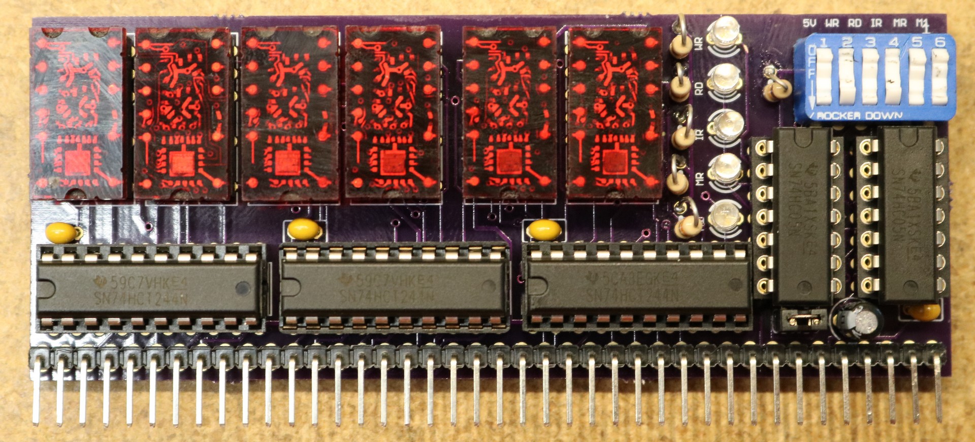
Here’s the assembled bus monitor board:

Z80 Bus Monitor Board, Assembled

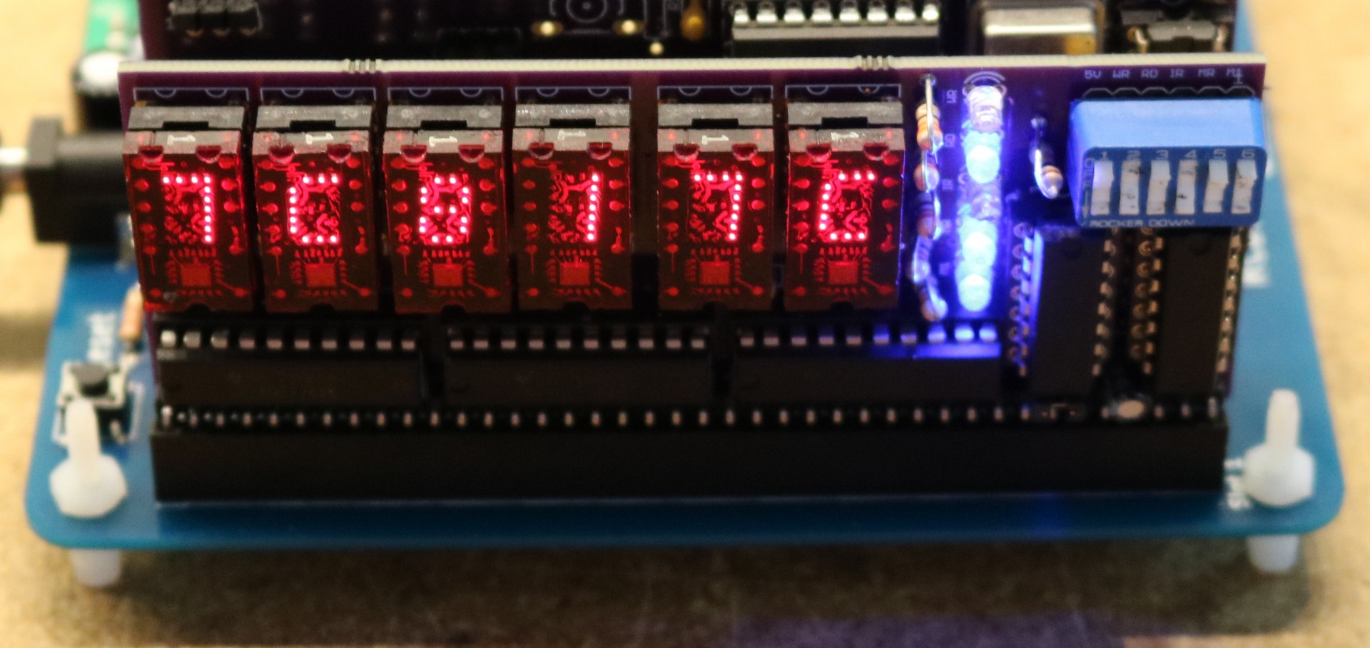
Finally, here’s a picture of the board in the front slot of the RC2014, displaying IO requests:

Busmon board, in use

One word of caution — these displays take a lot of current to run them. When I first plugged this board into my RC2014, I exceeded the capability of the un-heatsinked 7805 regulator and put it into thermal shutdown. I have since replaced the 7805 with a switching regulator from EZSBC.

Z80 Retrocomputing 4 – Bus Supervisor

$
0
0

This is the fourth in my series of Z80 retrocomputing blog posts.

For background, I suggest starting with the first post.

So what exactly is the purpose of the bus supervisor board? I wanted to do some assembly language work on the RC2014 Z80 Retrocomputer, and I examined several options:

  1. I could program an EPROM with my assembly language program, run it, then when it was time for the revision I could pop the EPROM out, erase and reprogram it, and repeat the cycle. I’ve done this before, and it’s a slow development cycle. You’re spending lots of time erasing and reprogramming EPROMs.
  2. I could write a bootloader and store that in the EPROM, and the bootloader could load a program from the serial port, or from an attached SD card, write that program to RAM, and execute it. This improves upon approach #1 by eliminating the need to erase and reprogram EPROMs. It requires some effort to local and/or write a boot loader.
  3. I could ditch the EPROM altogether, put some static RAM in its place, and come up with a way to program the static ram in-circuit.

The bus supervisor implements approach #3. I’m going to get rid of the RC2014’s ROM board, install a dual-RAM board in it’s place. Then I’m going to attach a raspberry pi to the Z80’s bus, let it put the Z80 to sleep, and have the pi program the RAM chip.

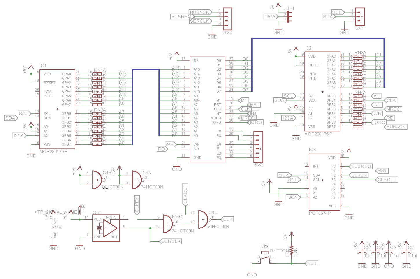
In order to seize control of the Z80’s bus, I’m going to use some io expander chips attached to the pi, and connect each of the Z80’s address, data, and control pins to the io expander. This will let the pi read and write those pins. Let’s see the schematic:

Z80 bus supervisor

Taking a look at the above schematic, we can see three IO expanders. Two are MCP23017 and one is a PCF8574. The MCP23017 are 16-bit IO expanders, and are by far the more versatile of the two chips, featuring configurable pull-ups, many different interrupt modes, etc. The PCF8574 is a much simpler chip and features only 8 bits of IO. We only need about 36 bits of IO to make this project work, so I opted to go with two MCP23017 and one PCF8574.

The MCP23017 and PCF8574 are both I2C devices, and they can communicate with the raspberry pi over a 3-pin (SDA, SCL, GND) i2c bus. I’ve used I2c in several of my projects. It’s really convenient and makes it easy to add peripherals to the pi.

As you can see, the entire address (A0..A15), data (D0..D7), and the majority of the control (M1, IORQ, MREQ, RD, WR, RESET, CLK, INT, BUSREQ, BUSAK) are connected to the IO expanders. They’re connected via some dip resistor packs. These aren’t necessary for correctness; they’re install to have some protection against operator error. If I program the MCP23017 incorrectly, then it would be possible to be outputting a “1″ on some pin while the Z80 is outputting a “0″, allowing current to flow in an undesirable way (perhaps burning out an IO line on one device or the other). The resistors limit the amount of current that can flow in the event of a mistake. I chose to use 470 ohm resistors, on the basis that it’s what I had in the junk box.

Also on the board is a clock generator. The supervisor board replaces the RC2014’s default clock board. The reason for this is twofold: 1) save on backplane space, and 2) to be able to stop the clock or implement a slow clock. I use a 7.3728 Mhz crystal oscillator, and it’s connected to a pair of NAND gates. If the CLKEN (PCF8574 output #3) signal is low then the on-board oscillator will be disabled. Outputting a squarewave on the CLKOUT (PCF8574 output #4) signal can then clock the Z80.
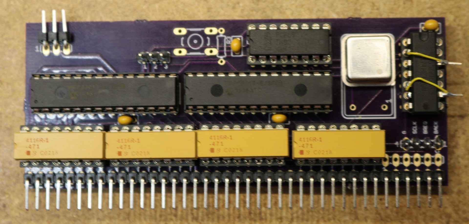
Here’s a picture of the completed Bus Supervisor board:

Z80 bus supervisor board for RC2014, assembled

It may be obvious (particularly from the little yellow wires) that there’s a few mistakes in the above board. These have already been corrected in the schematic. The next time I fab the pcboard (if there is a next time), I’ll correct the imperfections.

Seizing control of the Z80 bus

Okay now to the software… Our first task is to seize control of the Z80 bus. It’s handy that the Z80 provides a pair of pins for just this purpose. If we make BUSREQ low, then the Z80 will give up the bus, and everything important goes into tristate. Once it’s done this, it’ll set BUSACK low. Once we see BUSACK is low, the bus is ours to do with as we please. We need to reconfigure our MCP23017 io expanders so that the relevant pins are outputs instead of inputs. Then the pi can write to those IO pins.  For example, we can put an address on the address bus, set RD and MREQ low, and then read the data bus. That’s how we can examine a memory address.

In a similar manner, we can also write memory (set WR low instead of RD), and we can read and write IO ports (set IORQ low instead of MREQ). This allows the raspberry pi to interact with the Z80’s memory and IO devices.

We can dump a RAM chip by looping through all of the addresses, issuing a read of each one, and then writing the result to a file. We can do the reverse by reading a file, looping through all of the addresses, and issuing a memory write for each one.

When we’re done, we simply set BUSREQ back to high, and the Z80 will resume whatever it was doing.

Resetting the Z80

Since the PCF8574 io expander is connected to the reset pin, all we need to do to is set RESET low and then return it to high again.

Source Code

The source code for the supervisor program is available in my github repo at http://www.github.com/sbelectroncs/rc2014.

Z80 Retrocomputing 5 – Single Stepper for RC2014

$
0
0

In this blog post, I design a single step module for the RC2014.

[TODO: Insert Video Here]

If you haven’t read my introduction to retrocomputing yet, then please start there, as it describes the Z80 platform that I’m using.

The single step module is an alternative to the bus supervisor that I designed in the previous blog post. The bus supervisor implemented a slow clock, but it required a raspberry pi to do so. I wanted to design a module that required no raspberry pi, and added the ability to single-step and to auto-step the CPU. So why single step? Single-stepping is another feature that is handy for assembly language debugging. It allows you to execute exactly one instruction at a time. For each instruction, the CPU will wait for the user to press a button.

Auto-stepping is the other feature that this board implements. Rather than require the user to push the button, we can use a 555 timer to “push the button” for us. This makes the program run slowly, for example at a rate of 10 instructions per second or 100 instructions per second.

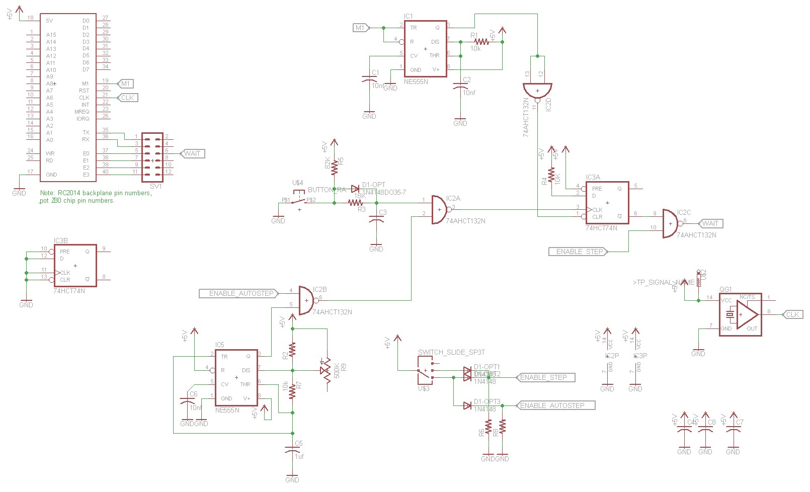
As the basis for my single stepper, I used this post at the Z80 Computer Project blog. It starts off with a circuit designed by Steve Ciarcia and published in his book Build Your Own Z80 Computer, which is available online. Ciarcia’s design uses a flip-flop to implement the single stepping. The M1 signal is fed into a one-shot and used as the clear signal for a 7474 flip-flop. The M1 signal clears the flip-flop, which sets the Z80 wait line low. This will cause the Z80 to wait until the wait line is set high again. A debounced pushbutton is used to clock a “1″ into the flip-flop, which will in turn raise the wait line and unblock the CPU. The next M1 cycle will clear the flip-flop and re-enter the wait state.

The Z80 Computer Project blog post replaced the monostable multivibrator used in Ciarcia’s circuit with a 555 timer. My modification replaces the SPDT step switch with a SPST pushbutton:

RC2014 single stepper schematic

One thing to note — both the Ciarcia book and Z80 Computer Project Blog showed the Pre input (pin 4) of the 7474 flip-flop unconnected. This caused chaos in my implementation. Sometimes it would work fine, other times the flip-flop would pick up noise and the wait pin would oscillate. I terminated pin 4 to 5V and the chaos went away.

The idea for the switch debounce came from The Ganssle Group’s blog post on switch debouncing. So what is switch debouncing? When you flip a switch or push a button, it doesn’t simply change from one state to the other, there’s a noisy phase where the state flips back and forth a few times as the metal is just starting to touch. This will glitch your typical DC logic circuit. So we need some circuit to filter out the noise and get us only the state change event from the switch.

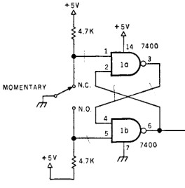
debounce circuit, from "Build your own Z80 Computer"

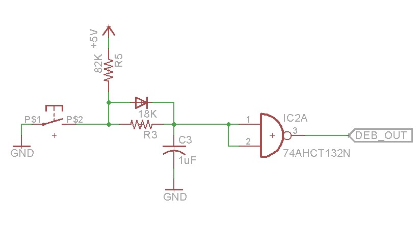
Ciarcia’s circuit used an SPDT switch and a couple NAND gates SPDT buttons aren’t super easy to find, and I wanted to use a SPST button. So I tried the RC schmitt trigger switch debounce circuit shown in the above schematic. The RC uses a network turns the noisy switch closure into a slower capacitor discharge, and the switch opening into a capacitor charge. Since it takes time to charge or discharge the capacitor, we eliminate the noisy spikes.

RC Schmitt Trigger Debounce Schematic

Note that the diode in the above schematic is optional, and is not necessary given the resistance values used above. The ganssle blog post gives the appropriate math.

The first time I built the circuit, I made the mistake of connecting the RC network to a plain ordinary 74HCT00 NAND gate. It’s important that you use a Schmitt trigger NAND gate,74AHCT132N. The Schmitt trigger includes hysteresis, which is necessary to prevent false triggering on the switch debounce. You can read more about Schmitt triggers on wikipedia.

The other change I made to the circuit is adding the autostepping feature. This is a second 555 timer configured as an oscillator. A NAND gate is used to enable or disable the output of the 555, and another NAND gate is used to combine the 555’s output with the pushbutton. Basically what happens is the 555 timer pushes the button for us. The values given in the schematic allow you to adjust the frequency from just under 1 Hz to around 100 Hz. It’ll depend on the specific capacitor you have as capacitors often have a fair amount of tolerance.

There’s a selector switch that lets you select “Run”, “Single”, or “Auto” modes.

Also on board is an optional 7.3728 Mhz oscillator. This allows the single step board to replace the RC2014’s clock board, saving a slot in the backplane.

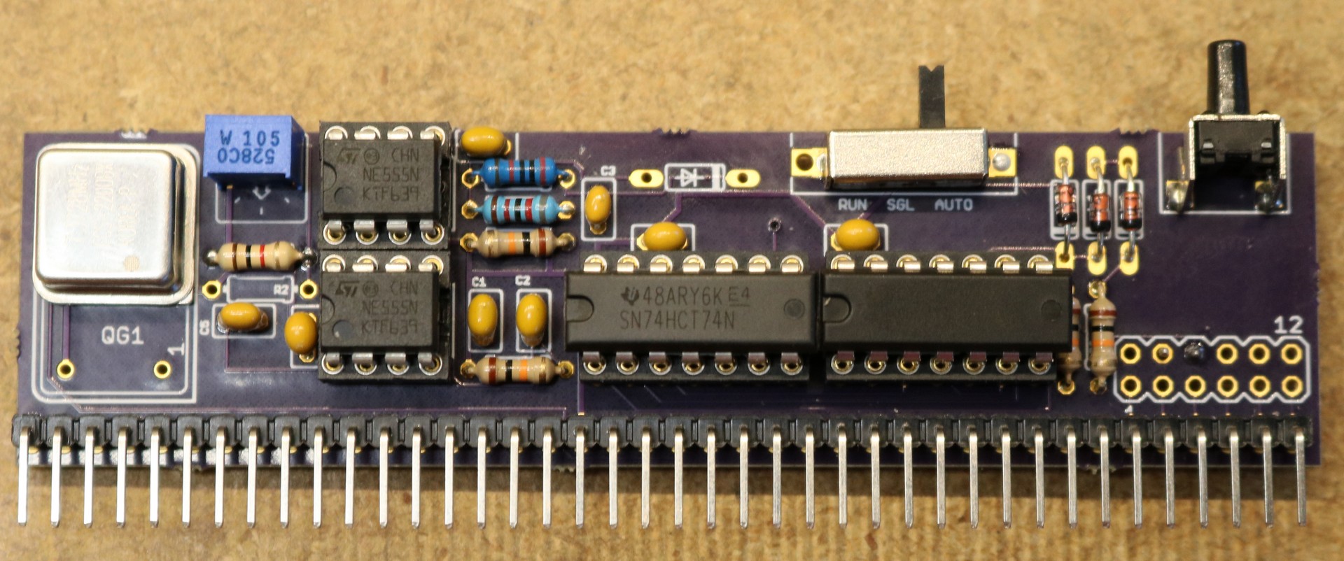
Here is a picture of the completed single stepper module:

RC2014 singlestep module, assembled

Viewing all 118 articles
Browse latest View live