In this video, I reverse engineer the protocol used by the HP 27201A.
The “major computer manufacturer” claim comes from the HP museum page for the SOM. There certainly were other speech synthesizers that were contemporary with this one, or perhaps even predated it. For example, the TI99/4A speech module. As such, I think it may come down to your definition of “major”.
Background
I bought this thing off ebay, not really knowing that much about it. The documentation on the web is really sparse, there’s basically on page and a half article that gives a few details.
HP Journal Article on the HP 27201A
The article was enough information to give me a couple of details:
The module is designed to sit inline, between an HP 1000 or HP 3000 series minicomputer and a peripheral device, such as a terminal or line printer.
The interface is RS-232 serial.
The communication protocol is ASCII, and has 8 commands.
Unfortunately, the details about the protocol were pretty vague. For example, although I knew there was a DOWnload command, I didn’t know the arguments or syntax.
Pictures
Below are some pictures of the speech synthesizer:
HP 27201A top viewHP27201A bottom viewHP 27201A front viewHP 27201A back view
It’s nice that the dip switch settings were documented right on the case, that would have made life a lot more difficult had they not been.
HP 27201A Inside View
The internal view we can see a lot of things:
A TMS5220 speech processor IC. Same chip as used by the popular TI99/4A speech synthesizer peripheral.
Five 2K static RAM ICs. This is where the speech data is stored. There are jumpers next to each IC that allow an EPROM to be placed instead. Using an EPROM would allow you to use pre-stored speech data rather than having to download it on startup.
A Z8 Microprocessor with a piggyback socket for a ROM. This is where the software for the speech module resides.
Two 8-pin RS232 line drivers, U11 and U13, UA9636ACP
A quad RS232 receiver, AM26LS32ACN
From the RS232 line drivers, it’s easy to learn which pin son the 15-pin connector are +12V and -12V. It’s also evident that four pins are RS232 output signals. From the AM26LS32, one can tell that there are four RS232 inputs.
Pinout
By tracing the pins, I managed to figure out the following:
Pin
Signal
1
Ground
2
Groond
3
Not Connected
4
+5V
5
SerIn 1B – Z8-P33, handshake line?
6
SerIn 3B – Likely serial RX from inline dev, passthrough to Pin15
7
SerIn 2B – Z8-P30, Serial RX (accepts escape sequences this pin)
8
SerIn 4B
9
Ground
10
+12V
11
-12V
12
Serout U11-2
13
Serout U11-1
14
Serout U13-2 – serial TX (probably to inline dev)
15
Serout U13-1 – serial TX (probably to host)
The key bit of information is that Pin7 is the serial input from the host and pin 15 is the serial output to the host. The other pins are either the slave device, which we don’t really care about, or handshake signals such as RTS/CTS, or power pins.
Reverse Engineering the Protocol
I pulled the ROM and downloaded it using my USB EPROM programmer and minipro software. Then using unidasm, a universal disassembler from the mame project, I disassembled the Z8 ROM.
Unfortunately, trying to understand an architecture your unfamiliar with, without any assembly comments or anything else to go on, can be a long process, and I stayed up two long weekend nights figuring out what arguments each of the commands took. This is what I came up with:
The download and speak commands are the most interesting. The first argument to each are two decimal numbers separated by a dot, which identify a bank and phrase. For example, 3.27 would be RAM chip #3, phrase #27. The bank numbers start at 1.
When downloading, you then specify the length in bytes. Then you put the letter F or V (no, I don’t yet know the difference) and finally you send a bunch of hex bytes, two characters per byte. Separators between the hex bytes are not necessary.
Every command (except identify, which isn’t really a command) is terminated with a semicolon.
The Status, Upload, and Identify commands for me all did not produce output unless I followed their escape sequence with an <XON> character.
Obtaining speech data
Bitsavers has a collection of HP 1000 software, and the Voice Exerciser (VX) program that would have originally been used with the speech module is present there in the type-4 and type-5 archives. Specifically, this list of files. The 27203 files are the ones you’re looking for:
The two files with the speech data are 27203-16007_Rev-2330.src and 27203-16009_Rev-2320.src. These two files together contain approximately 1700 English words and their associated speech data.
Note that the VX software could be run on an actual or simulated HP 1000 series computer and that would have yielded the protocol by simple snooping of the serial interface. That was my backup plan had I been unable to disassemble and understand the Z8 ROM. I did have a lengthy chat with Dave Bryan who developed the Simh HP2100 simulator, and learned that loading complex software that requires a database, such as the voice exerciser, may be a daunting project. It’s still my hope, with some help from Dave, that I might be able to get this running on the simulator and try it out in the environment it was intended to work in.
My python program
I wrote a python program to communicate with the speech synthesizer and it’s present in my github repository linked below. There are two programs:
build_vocab.py. Builds a vocabulary file to download to the module, acceptings words from stdin and writing the vocabulary to stdout.
hpcli.py. A command-line tool to interact with the speech module, with commands for initializing, speaking, etc.
The video at the top of this blog post shows me running the python programs to interact with the SOM
In this post, I create a floppy controller for my raspberry pi model 4 B.
Purpose
If there’s one criticism I hear more often than any other about the pi, it’s “I wish my Raspberry Pi had a floppy drive“. It’s really shocking that the pi doesn’t have the ubiquitous 34-pin floppy header that we all know and love. How else are you supposed to interface your Tandon TM100-2A or your Teac FD-55BR or even, for you cutting edge folks, your Sony MFP290 3.5” high density drive?
So I set along to create this much needed had, the missing link between the raspberry pi and the floppy disk drive.
Design
I’ve used the WD37C65 floppy controller IC a few times in the past, most notably as part of a floppy interface project for the RC2014 computer. I’ve previously played with the RomWBW CP/M distribution for the RC2014, and the floppy drive that’s contained as part of it. So I knew this chip reasonably well and decided to go ahead and make use of it for my raspberry pi project.
The WD37C65 is a great single-chip solution, combining the floppy controller, data separator, and control latch. It actually has three different chip selects, one for the controller, one for the DOR (disk operation register?) and one for the DCR (disk configuration register?). You can easily interface it with a plethora of vintage drives, everything from your basic 360KB floppy drive to your 1.44 MB high density drive. Yes, I’m pretty sure when working on the RC2014 I interface it to some old 8″ qume drives as well. There are several selectable data rates, and you can program the number of tracks, number of heads, number of sectors, and bytes per sector. The controller can be used with an interrupt or it can use polling. It’s a great vintage IC to use.
Here’s my schematic for the raspberry pi floppy controller hat:
Raspberry Pi Floppy Drive Controller Schematic
The circuit is really pretty simple, there’s only one IC, the WD37C65 controller. This IC connects directly to the 34-pin floppy header. There are also some pullups associated with about a half-dozen of the floppy drive status lines, things like the index sensor and the write protect sensor. There’s a 16 MHz oscillator that supplies the clock that the controller needs.
Most of the controller lines are interfaced directly to the pi. Lines like RD, WR, CS, A0, etc., are strictly pi-to-controller signals and both the pi and the controller are compatible even though the pi is a 3.3V device and the controller is a 5V device.
The data bus, D0-D7 is a bit more controversial. The signal levels are compatible when the pi is writing to the controller (3.3V -> 5V), but are not necessarily compatible when the controller is writing data to the pi (5V – 3.3V). When doing that sort of thing on a hobbyist-grade device I’ll often throw in some current limiting resistors. That’s the purpose of the resistor network RN3. In my video I did actually test it wired straight across, and damaged neither the pi nor the controller, though it may be risky to do so. As far as I’m aware, there isn’t a great deal of real-world studies on interfacing a pi with 5V devices, other than a lot of people saying “don’t do it”. For the next revision of this board, I’ll probably switch to using a proper level converter IC and eliminate the controversy.
I put two additional headers on the board, one for I2C and the other for serial. These fit some use cases I have planned for the board.
Implementation
Below is a picture of the completed hat:
Raspberry Pi Floppy Controller PCBOARD, Assembled
As you can see, a pretty simple one-chip hat. The 16-pin grey thing is a shunt. This is the configuration I used in the video. As I mentioned in the design section, perhaps safer here to use a DIP resistor network (isolated, not bussed) or solder in discrete resistors due to the level difference between the pi and controller IC.
The floppy header is at the bottom. If you get the shrouded header like I did, with the little cutout in the middle, it’ll keep you from pulling in your floppy cable backwards.
The stacking header for the pi protrudes out the back.
The barrel jack is optional and would allow you to supply 5VDC from a barrel jack instead of the pi’s USB-C header, if you’re a barrel jack sort of person. If you’re one of those modern USB-C people, then just use the USB-C.
Software
I wrote a user-mode driver in python, with C extensions for some of the IO functions. This presents a couple challenges:
Raspbian is not a real-time OS. There’s no guarantee that your user-mode process will not be interrupted.
When transferring data (i.e. read sector or write sector), the floppy controller wants every byte transferred within 13ms (standard density) or 26ms (high density). If you don’t transfer the byte in time, the controller have no place to put the next byte — the disk is spinning! — and will declare an overrun.
These two together mean that a user-mode floppy driver may have occasional overruns. No problem, when we get an overrun, we can just retry. It does have an adverse affect on performance though, and the problem is much worse when reading high density disks than when reading low density disks.
Some techniques at https://www.raspberrypi.org/forums/viewtopic.php?t=228727 can be used to mitigate the problem. By dedicating a core to the floppy driver you lose a core from general purpose use, but you also reduce the odds of Linux interrupting the floppy driver at an inopportune time. An interrupt may still occur, but less often and with less adverse affect than when sharing a core with other processes.
The ultimate solution would be to write a kernel driver. I’ve written kernel modules in the past. Perhaps it’s something I will do again, but I have no immediate plans to do so.
Demo Script
Here is a list of commands I performed in my short demo in the video:
# format the diskette
sudo python ./fdtool.py --media 360 format

# write a DOS 3.10 image to the disk
cat dos310_1.img | sudo python ./fdtool.py --realtime --pincpu 3 --media 360 --disk write

# Read the first sector and display it in the terminal
sudo python ./fdtool.py --realtime --pincpu 3 --media 360 read | hexdump -C

# Read the entire disk and display it in the terminal
sudo python ./fdtool.py --realtime --pincpu 3 --media 360 --disk read | hexdump -C
Note that the sudo goes along with the --realtime --pincpu 3 arguments and handles pinning the floppy controller to cpu core #3. It’s also necessary to add isolcpus=3 to your /boot/cmdline.txt. It will work without the sudo and without the pinning arguments, but you’ll get more interruptions and more retries needed.
My github repository at https://github.com/sbelectronics/smb-pi-lib contains a library of my frequently used code, including the floppy driver and the driver’s C extensions.
Acknowledgements
The RomWBW CP/M assembly floppy driver, fd.asm, served as a basis for much of my learning how to program the WD37C65 and a basis for writing my python driver.
In this video, I put together a T5745 thin client with a PCI expansion adapter and a GPIB adapter.
Background
I’ve started playing with some HP 9000 computers, both the series 200 (9836, 9920, etc) and the series 300 (model 310). With a few exceptions such as the 9836, these computers often don’t include built-in storage. They have an HPIB interface, using IEEE-488, that connects to one or more external storage devices. Common storage devices are the 9121 and 9122 floppy drive units, the 9134 hard drive, or the 9133 which is a combination floppy and hard drive.
While you can successfully find these storage devices on eBay, they’re still not all that convenient to use as you would have to preload them with the appropriate image that you want to use.
Along came HPDrive, a project that can turn any old Windows or Linux computer into a HP-compatible drive using a GPIB adapter. Unfortunately, most of the GPIB adapters are old ISA and PCI cards. There are a few newer PCIE cards, an some USB Adapters, though the USB adapters are not well supported by HPDrive at this time. Although I do have some ISA machines (Xi8088, PC 5150, etc), these are fairly large builds that I didn’t want to dedicate to serving as a HP storage device.
So I set about building the smallest affordable HPDrive computer that I could.
HP9000/310 computer connected to T5745 thin client running HPDrive
The T5745 Thin Client
This brought me to the T5745 “thin client”. You can find these readily on eBay. It typically comes with an Atom N280 processor, 1 GB of memory, VGA video, and a typical assortment of USB and PS2 ports. This is just about the right solution for running a relatively small Linux distribution. The one thing the T5745 is missing is an expansion card slot — it doesn’t have a PCI or PCI Express slot.
However, there are new “expansion chassis” available on Amazon, for a modest fourteen bucks (what can you buy for 14 bucks shipped these days??? A T5745 thin client expansion chassis, that’s what…). When looking for this, search for “Hp T5740 Thin Client Az551aa PCI Express Expansion Module Chassis – 581264-002“.
This expansion chassis comes prepopulated with a PCI Express card adapter, but it also includes a PCI adapter that can be swapped in. Be careful buying it on eBay as some eBay listings include only the PCI Express adapter. It also has serial and parallel ports and a small fan. The first step is to swap the PCI Express adapter board with the included PCI adapter board.
Strangely, the PCI board doesn’t include a header for the fan, so you can toss the fan if you want. Perhaps the PCI Express specification allowed for higher-wattage components that needed active cooling, whereas maybe PCI does not. Or perhaps the fan interfered with the typical PCI card form factor. Regardless, I left the fan unconnected.
I did have to do a little bit of surgery (with a wire cutter and pliars) on the expansion chassis where part of the metal was interfering with the relatively large HPIB cable connector. A dremel would have made cleaner work of it.
NOTE: Some thin clients you find on eBay do not include the power brick. Plan to pick one up, build your own, or repurpose a power brick from another piece of equipment. My power brick is an HP-branded one, with the label “U1000EA”. It measures 19.5V on my bench fully unloaded using a multimeter. I bought it under the eBay listing “GENUINE HP Thin Client T510 T5565 T5570 T5740 T5745 65W AC Power Supply Adapter”.
Selecting a GPIB Card
The HPDrive documentation has a list of acceptable models. I went for a National Instruments PCI-GPIB Card. The specific listing I used had the title,
That listing on eBay is now out of stock, but I’m sure you can find similar NI PCI-GPIB adapters.
Storage
The T5745 I received did not have any storage, but it did have an internal unpopulated IDE header. This header is for a disk-on-module, such as the Transcend TS4GDOM44H-S. My speculation is the thin clients originally came with a DOM module like this, but perhaps it was removed for data security reasons. Using something like the transcend will return the thin client to the original design. Alternatively, the T5745 has multiple USB ports, including two USB ports that are conveniently hidden inside the case, where USB storage could be plugged in.
Installing Ubuntu
Next I installed Ubuntu 16.04. I chose 16.04 because I needed a 32-bit variant for the atom N280 processor. Newer 64-bit versions of Ubuntu will not work.
Ubuntu installs from a USB thumb drive. You put the USB stick in the desktop machine of your choice (I used my Windows 10 desktop), and then run a USB image burning tool to burn the Ubuntu image to a USB stick. You can then use this USB stick as installation media on the thin client. I think I probably used “balenaEtcher” to burn the USB image, though I’m not 100% certain. There are several alternative programs that could be used.
My first install was a little bit problematic as I ran out of disk space shortly after installing. The transcend DOM only has 4GB of storage space, and Ubuntu 16.04 will eat up a huge chunk of that. I reinstalled and reduced the size of the swap partition substantially (down to 0.3GB). We don’t really need swap in such a small deployment like this, and I was able to free up a significant amount of space. An alternative as described previously would be to use a USB thumb drive instead of the transcend module. You can easily get USB thumb sticks in the 32 GB or 64 GB range, which would have plenty of space.
We don’t really need swap in such a small deployment like this, and I was able to free up a significant amount of space. An alternative as described previously would be to use a USB thumb drive instead of the transcend module. You can easily get USB thumb sticks in the 32 GB or 64 GB range, which would have plenty of space.
My notes show that I had to fuss with some grub settings to get Ubuntu 16.04 to boot. This is what my notes say:
# If Ubuntu hangs during "free smp alternatives memory", boot
# using recovery mode and do this:
sudo emacs /etc/default/grub
GRUB_CMDLINE_LINUX="dis_ucode_ldr"
sudo update-grub
YMMV, but that’s what I had to do.
Building the Linux GPIB Driver
Here you want to follow the Linux instructions in the HPDrive README.
NOTE: The commands I use below might not necessarily be the same as what you’ll do depending on specific hardware. I suggest you read and understand the HPDrive documentation. My commands are listed as a reference.
The first thing I did was to install the right kernel:
# Download and install the kernel that HPDrive wants...
wget https://kernel.ubuntu.com/~kernel-ppa/mainline/v4.0.3-wily/linux-headers-4.0.3-040003-generic_4.0.3-040003.201505131441_i386.deb
wget https://kernel.ubuntu.com/~kernel-ppa/mainline/v4.0.3-wily/linux-headers-4.0.3-040003_4.0.3-040003.201505131441_all.deb
wget https://kernel.ubuntu.com/~kernel-ppa/mainline/v4.0.3-wily/linux-image-4.0.3-040003-generic_4.0.3-040003.201505131441_i386.deb
sudo dpkg -i *.deb
Then I updated grub to automatically boot to that kernel:
grep submenu /boot/grub/grub.cfg
grep gnulinux /boot/grub/grub.cfg
sudo emacs /etc/default/grub
# Inside emacs, put a > between the two ids grepped above
GRUB_DEFAULT="gnulinux-advanced-98f2e22d-949b-4de9-96f6-ffb1c380bed2>gnulinux-4.0.3-040003-generic-advanced-98f2e22d-949b-4de9-96f6-ffb1c380bed2"
sudo update-grub
Reboot, make sure it boots cleanly, and make sure that “uname -a” shows the same kernel that you installed. Then I built the driver.
sudo apt-get install build-essential

wget https://sourceforge.net/projects/linux-gpib/files/linux-gpib%20for%203.x.x%20and%202.6.x%20kernels/4.0.3/linux-gpib-4.0.3.tar.gz/download -O linux-gpib-4.0.3.tar.gz
tar -xzf linux-gpib-4.0.3.tar.gz
cd linux-gpib-4.0.3
# Assumes this file is in the parent directory; it comes from HPDrive
cp ../linux-gpib-4.0.3.patch .
patch -p1 < linux-gpib-4.0.3.patch

./configure
make
sudo make install
Next, configure the gpib driver to match your board (your board may differ from mine; pay attention to the HPDrive instructions about seeing what your drive’s ID is):
sudo emacs /etc/gpib.conf
# insert the following configuration using emacs
interface {
        minor = 0       /* board index, minor = 0 uses /dev/gpib0, minor = 1 uses /dev/gpib1, etc. */
        board_type = "ni_pci"   /* type of interface board being used */
        name = "gpib0"  /* optional name, allows you to get a board descriptor using ibfind() */
        pad = 21        /* primary address of interface             */
        master = yes    /* interface board is system controller */
        pci_bus = 1
        pci_slot = 6
}

sudo modprobe tnt4882
sudo /usr/local/sbin/gpib_config --minor 0
The HPDrive documentation will have you run a command or two to ensure that the driver is working as expected, and that the software connects to the driver.
Optional — Setting up a Pi-KVM to interact with your HP 9000 Computer via your modern PC.
One of the things I show in the video is the use of a Pi-KVM. I like doing this because it allows me to play with a piece of retro equipment over from the convenience of my comfortable desk, using my big monitor and my nice keyboard. I prefer this to having to scrounge up an old CRT tube, buy an overpriced old keyboard, etc.
HP9000/310 computer connected to PiKVM
The pi-kvm website will walk you through building a Pi-KVM if you want to follow in my footsteps.
For an HP 9000 series computer, you’ll probably also need a scan converter. For my 9920 and my 9000/310, a GBS-8219 scan converter worked perfectly. This will take the single-RCA composite connector and output VGA video (which you can in turn feed to the Pi-KVM or to the VGA monitor of your choosing). A GBS-8200 will also suffice and can be had cheaper than a GBS-8219.
The video on a HP9836 was a bit more troublesome to deal with, and I ended up hacking an MCE2VGA board. But that’s a story for a different blog post…
To use a modern keyboard, or to use the Pi-KVM’s emulated keyboard, with a 9920 or 9000/310 or similar 9000 series computer, you’ll have to go through a few more hoops. The really old ones (9920) use a weird proprietary clocked shift protocol. The newer ones (9000/310, etc) use HP-HIL, which is at least reasonably well documented. Fortunately, Anders Gustafsson has developed PIC-based converters for both of these computer over to the USB HID keyboard protocol. I’ll leave you to Anders’s site to work out how to do this, though I’ll probably document my setup in a future blog post.
In this post, I build a Basic Flash and RAM board the the HP 9000 series of computers:
Purpose
Lately I’ve been playing with old HP computers such as the 9836, 9920, and 9000/310. These computers typically do not come with ROM basic or any other ROM operating system. Without a ROM board, you have to boot off disk, either a floppy or an attached hard drive. There were ROM boards back in the day, but if and when you encounter them on eBay, they can be pricey. So I decided to make my own.
Background / Research
I started by looking around at the HP Museum, and found references that Dominique Berget had documented the schematics and reverse engineered and reproduced the Basic 4.0 board. I contacted Dominique and asked him a few emails — he sells completed boards, but not kits or bare pcboards. He provided me with some additional schematics, links to the ROM images, and advice on creating my own board. It seemed simple enough to do so, so I set out to design and fabricate my own boards. While the first one more-or-less worked, it took me about four revisions to finally get the design to the point I was happy with it.
The HP Dio Bus
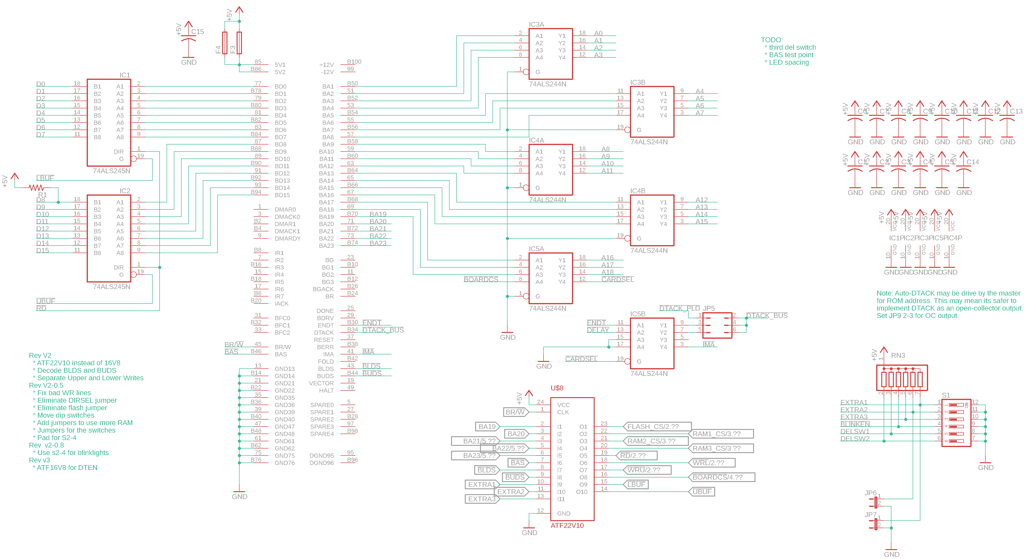
The Bus used on the HP 9000 200 and 300 series is called “DIO”, and you can find some specifications for it on the web, including even schematics for how typical memory and peripheral boards are implemented. Typically, an expansion board buffers everything — 74LS244 buffers are often used for unidirectional signals such as address lines, and 73LS245 buffers are used for bidirectional signals such as data lines. The bus is 16-bit, and includes a pair of signals, BLDS and BUDS that tell you whether to read/write the upper or lower 8-bits. Reading or writing both the upper and the lower 8-bits at the same time is common, especially for memory boards. There is an IMA signal that is used by the expansion board to indicate that an address has fallen into the board’s address space, and a DTACK signal that indicate when a transfer is complete.
Designing a ROM, Flash, or RAM board is as simple as the following:
Buffer all of the address bits.
Decode the address to determine whether your board is addressed.
Assert the appropriate data buffers for lower or upper transfers, and set them to the proper direction (read or write)
Assert IMA to indicate that you board is handling the request.
Transfer the data
Assert DTACK when you’re done.
In my experience, DTACK is where all of the complexity comes into play. There was actually a movement back in the day, “DTACK Grounded” that asserted you could simply ground the line, and if memory was fast enough, everything would just work. I’m not sure if this would work on the 9000, but to do it to spec needs some additional work.
Some computers, the 9836 and 9920, will automatically assert DTACK for you, for some addresses. More than anything I found this a bit annoying, as it complicates the implementation (which computer do I have? Is my board outside the auto-dtack space or inside it?).
There’s an ENDT (“Enable DTACK”) line asserted by the processor that you can use. If your card is selected, then you can simply pass ENDT through to DTACK, and you will end up asserting the DTACK about 5 cycles into the transfer.
However… if you have a DMA board such as the 98620A or 98620B, the DMA board will perform memory transfers but it will not generate ENDT. The DIO specification says that every board that can accept ENDT must also work if ENDT is not implemented. For this reason, as a fallback you need to implement your own delay line.
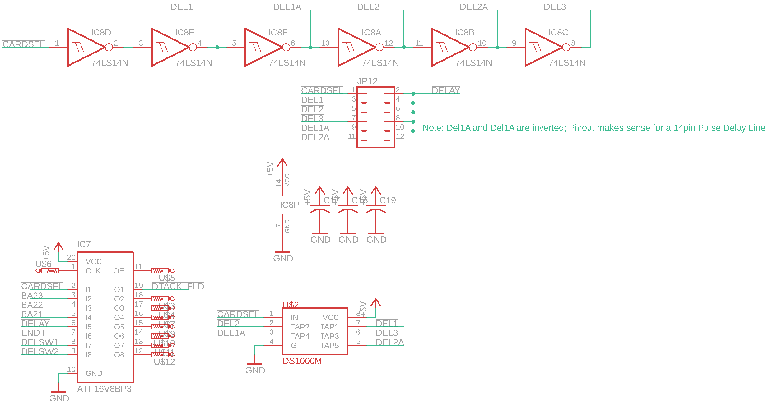
Schematic
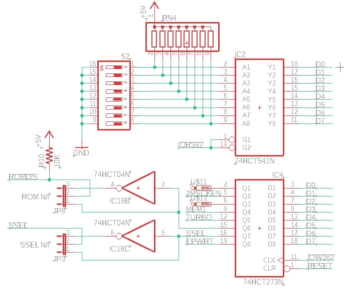
Below is the schematic for my board. Let’s go through it a page at a time. Click any of the schematic pictures to get a decent size view.
HP 9000 Flash / RAM Board Schematic, Buffers and Logic
Above we have the standard buffering arrangement. There are two 74ALS245, one each for the upper and lower data bytes. There is a separate enable to drive each one of them, and a direction that is common to both of them. For the address lines, there are a plethora of 74ALS244 which are always enabled and unidirectional. There is half of a 74ALS244 left over, so it gets used to drive the IMA signal. The ‘244 is a tri-state device, when it’s not enabled IMA can float. When the device is enabled, the ‘244 will drive IMA low. This half of the ‘244 also gives us our first option to implement DTACK — by selecting the second position of JP5, we can drive DTACK based on ENDT. By selecting the third position of JP5, we can drive DTACK based on a delay. Don’t try to use both positions at the same time — we’ll get to that later.
An ATF22V10 handles all of the decoding logic. It decides when the board is addressed, which RAM or Flash chips to select, when to enable the upper or lower buffers, etc. This device needs to be programmed, and can easily be programmed with a TL866II. Note that the original TL866 will not program the ATF22V10.
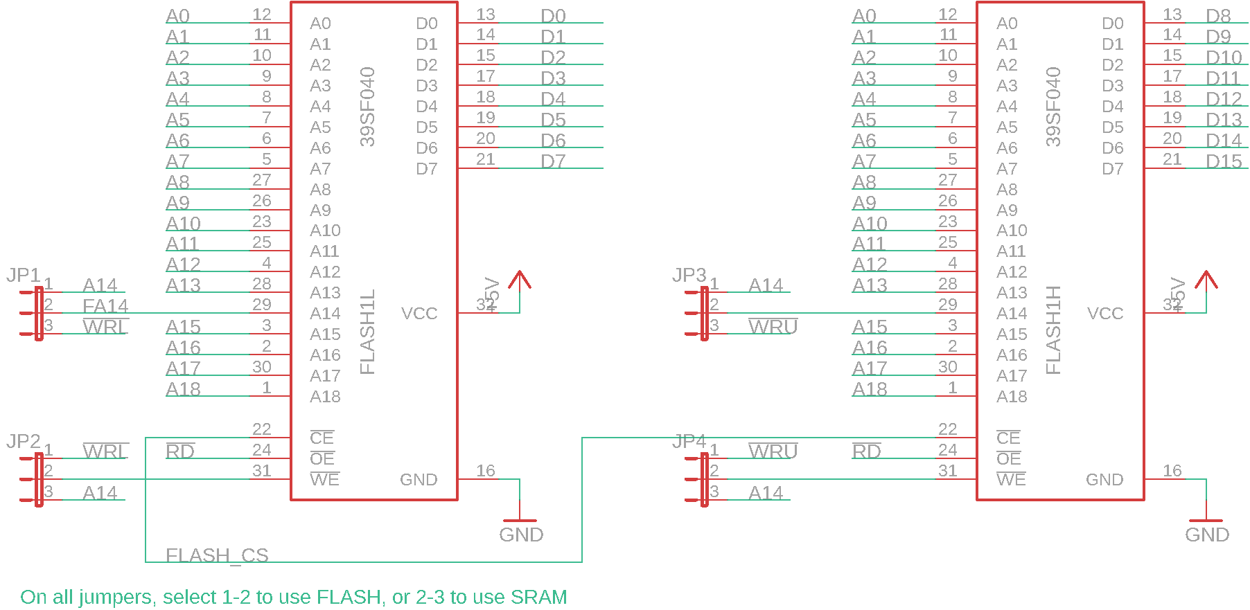
The next page is for the Flash ICs
HP 9000 Flash / RAM Board, Flash ICs
The above is simple enough, it’s just two 39SF040 flash memory ICs. Recall this is a 16-bit bus, so to use 8-bit memory devices like the 39SF040, we’ll need two ICs, one for upper and one for lower. The four jumpers allow you to switch these sockets between the pinout for a 39SF040 and an AS6C4008 memory IC. The pinouts of those two devices are almost identical, but annoyingly not quite identical. By moving the jumpers, you can change the board from a hybrid flash + RAM board to a board that implements all RAM. Next up are the RAM IC sockets.
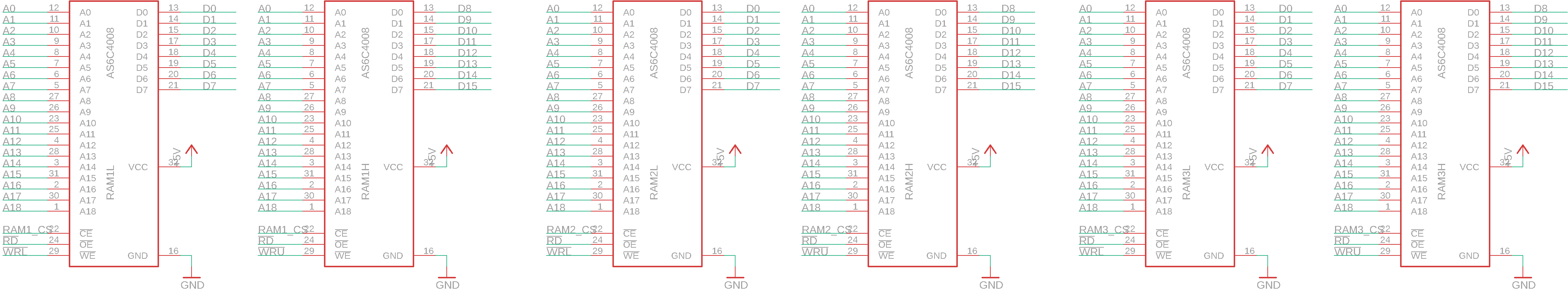
HP 9000 Flash / RAM Board, RAM
The RAM sockets look much like the Flash sockets. There’s 6 of them, 512KB each, for a total of 3MB. Again note that the upper and lower ICs are selected separately. Next let’s have a little fun!
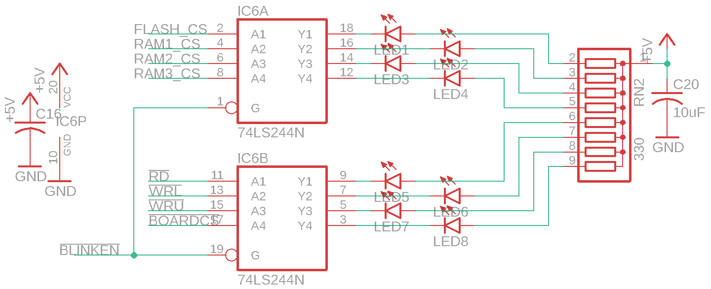
HP 9000 Flash / RAM Board, Blinkenlights
Everybody likes blinky lights! Here I used another 74ALS244 IC to drive the LEDs. They’re connected to the chip selects for each of the memory backs, the RD and WRT strobes, and the board chip select. The lights aren’t merely frivolous; I did use them to diagnose the earlier versions of the board. When the computer is booting and doing the memory check, you can see each of the CS lines light up in turn.
Finally, one last bit of complexity…
HP 9000 Flash / RAM Board, Delay Circuit
As I mentioned previously, the DIO specification insists that using ENDT to trigger DTACK is not sufficient. Every board must also be able generate DTACK even if ENDT is never asserted. This is necessary to function correctly with the (optional) DMA board. There’s also the nit about AUTO-DTACK, that the computer may be asserting DTACK for certain addresses.
For this, I added another PLD, this time a slightly smaller ATF16V8. The primary function is as a fancy OR function — it can assert DTACK if it sees ENDT asserted, or it can assert it after a fixed delay. The ATF16V8 can be configured to support a tri-state output, which is perfect for the bus specification. Finally, it also pays attention to the upper 3 address bits and can be configured to avoid asserting DTACK in the range where it thinks the CPU will be doing auto-DTACK.
To generate the actual delays, I used a 74LS14N schmidt trigger inverter. This device has a relatively reliable delay of about 15ns per gate. If you put jumper JP12 in the second position, you should get about 30ns of additional delay. If you put it in the third position, you’ll get about 60ns of additional delay. However, in my tests, I found that using the 74LS14 was not necessary — there was sufficient delay already in the other logic circuits (the ATF22V10, the 74LS244 buffers, etc) that I was able to jumper JP12 in the first position, which is zero additional delay. That would be my default suggestion — leave IC8 unpopulated and put JP12 in the first position. If it gives you trouble, then populate IC8 and move the jumper to the second position.
U$2, a DS1000M was an alternate footprint for an alternate purpose-built delay IC. They’re not made anymore, but some can be found on eBay. Ultimately it was not necessary and can be safely ignored.
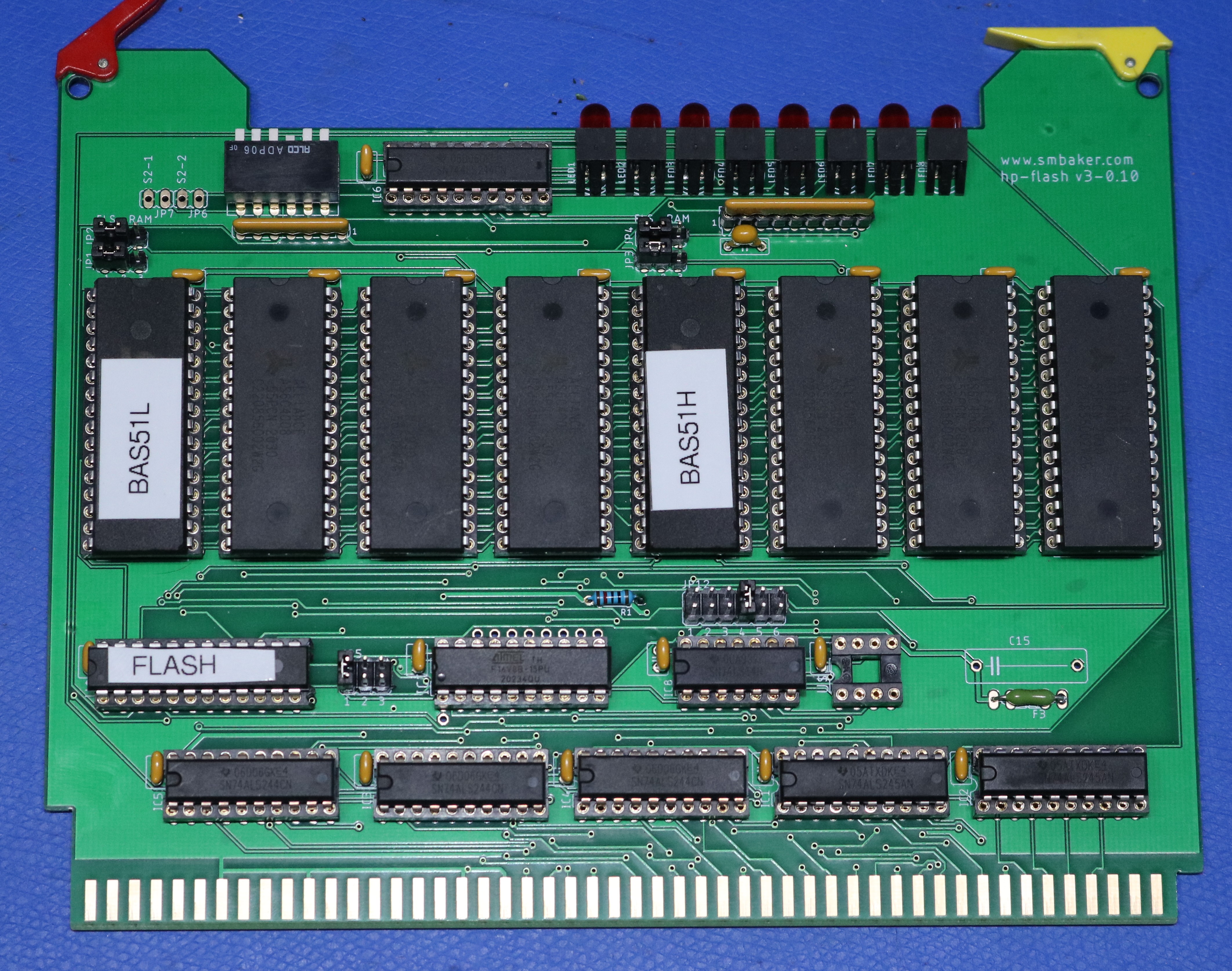
Implementation
Below is a picture of the board.
Completed HP 9000 Flash and RAM Board
The implementation is rather straightforward — above you can see the two flash ROMs with white labels on them, BAS51L and BAS51H for lower and upper respectively. The other large ICs are the RAM chips. The 22-pin narrow DIP is the PLD device. JP12 is in the 90ns delay position; this photo was taken before I realized I could jumper it to the 0ns position.
I opted to go with a right-angle dip switch. This makes it easy to adjust the board while it’s mounted in the case. The little red and yellow ejecter levers were scavenged from a 256K HP RAM board.
Resources
TODO: Work in progress… Put up the github repo link…
In this post, I make a battery-operated Wifi trigger to turn on the master valve for my sprinkler system.
Purpose
The way the pipes are configured for the sprinkler system, there’s a master valve in front of the yard hydrant that I use for my garden hose (there are reasons for this, but they are due to plumbing, not due to electronics!). I have a RainMachine smart sprinkler system controller, so I can easily trigger the master valve from my phone or ipad. However, I don’t always have my phone on me, and it’s an extra step to open up some app and login just to be able to turn on a faucet. So, I put together this ESP8266-based remote control.
Operating an ESP8266 off batteries
The ESP8266 has a “deep sleep” mode that consumes a very low amount of power. The basic idea is to execute the tasks you need inside the setup() routine for your arduino sketch, and then enter deepsleep at the end of the setup routine. The loop() function is empty. The button is then tied to the reset of the ESP8266. Pressing the button causes a reset, which in turn causes the setup() routine to run again, and then sleeps. So the first part of the problem, minimizing energy consumption is relatively simple.
Next, we have to figure out how to safely run an ESP8266, which is a 3.3V device, off of batteries. A few projects I encountered ran the ESP8266 ESP-01 module directly off a battery, either 3.7V lithium chemistry, or a trio of AA/AAA batteries (which could be anything from alkaline to nimh). The problem with any of these approaches is that you’re subjecting the ESP8266 to a voltage that is outside of its operating specification. Batter voltage can vary wildly; a battery you think might be 3.7V nominal might be a bit higher than that fresh off the charger. While I’m sure these other projects worked fine, I felt it safer to use a regulator. The MCP1700-3302E regulator was recommended by a few projects on the Internet.
Schematic
The schematic is simple, bordering on trivial.
Battery Operated ESP8266 Wifi Button
Note that the 1000uF capacitor is perhaps a bit overkill — the datasheet calls for 1uF, which may well be sufficient. I grabbed something random from the junk box without really thinking about it, and also grabbed something I felt would smooth out any high current spikes from the module while it’s performing its RF operations.
The MCP1700-3302E is a low-dropout regulator that has a low quiescent current. Checking the circuit while in deepsleep using my EEVBLOG uCurrent Gold showed the approximately 20-25 microamps consumed.
Implementation
Here are some pictures of the build…
ESP8266 Wifi Button Mounted in Case
No custom pcboards here. I assembled the regulator and it’s capacitors by soldering the components and wires together. Then I gunked them up good with the hot melt glue gun. The battery holder came from amazon — it’s a quad AAA holder with one of the slots wired across. The button also came from Amazon, the result of a search for “waterproof button” (which I’m not entirely convinced is waterproof; we’ll see). The blue case is an “S3 T2000 Watertight Case”, which I’ve used in a few previous projects.
I’m starting a new project, an IDE adapter for the Epson QX-10 computer.
Someone did this in 1995…
Some very old posts by Wayne Sung and John D Baker give me some hope this is possible:
A couple of years ago, I was involved in the development of a control chip for a system-independent IDE host adapter. In my case, I built an adapter for my Epson QX-10 to use an IDE hard disk. The interface was fairly simple to build and only minor changes to the BIOS were necessary. The old WD1002-HDO driver routines were 95% correct for controlling the IDE hard disk (first a Conner CP-3022, then a Conner CP-342, and now a Conner CP-3024). For the record, the only changes made were: Add 1 to the sector number (IDE starts at sector 1, not 0 [=256]). Explicitly request a 1-sector transfer. In the process of making the changes, the old explicit seek code had to be eliminated, but since IDE drives perform implicit seeks on all commands, no functionality was lost. If you are interested in building an IDE host adapter for your favorite 8-bit machine, you can obtain a system-independent control chip and general schematic from:
These posts are quite old (circa 1995) if anyone would happen to know Wayne or John, that would be a big help. On the wayback machine, I was even able to find a couple pictures of Wayne hand-made IDE adapter.
Taking a look at the Comrex Comfiler
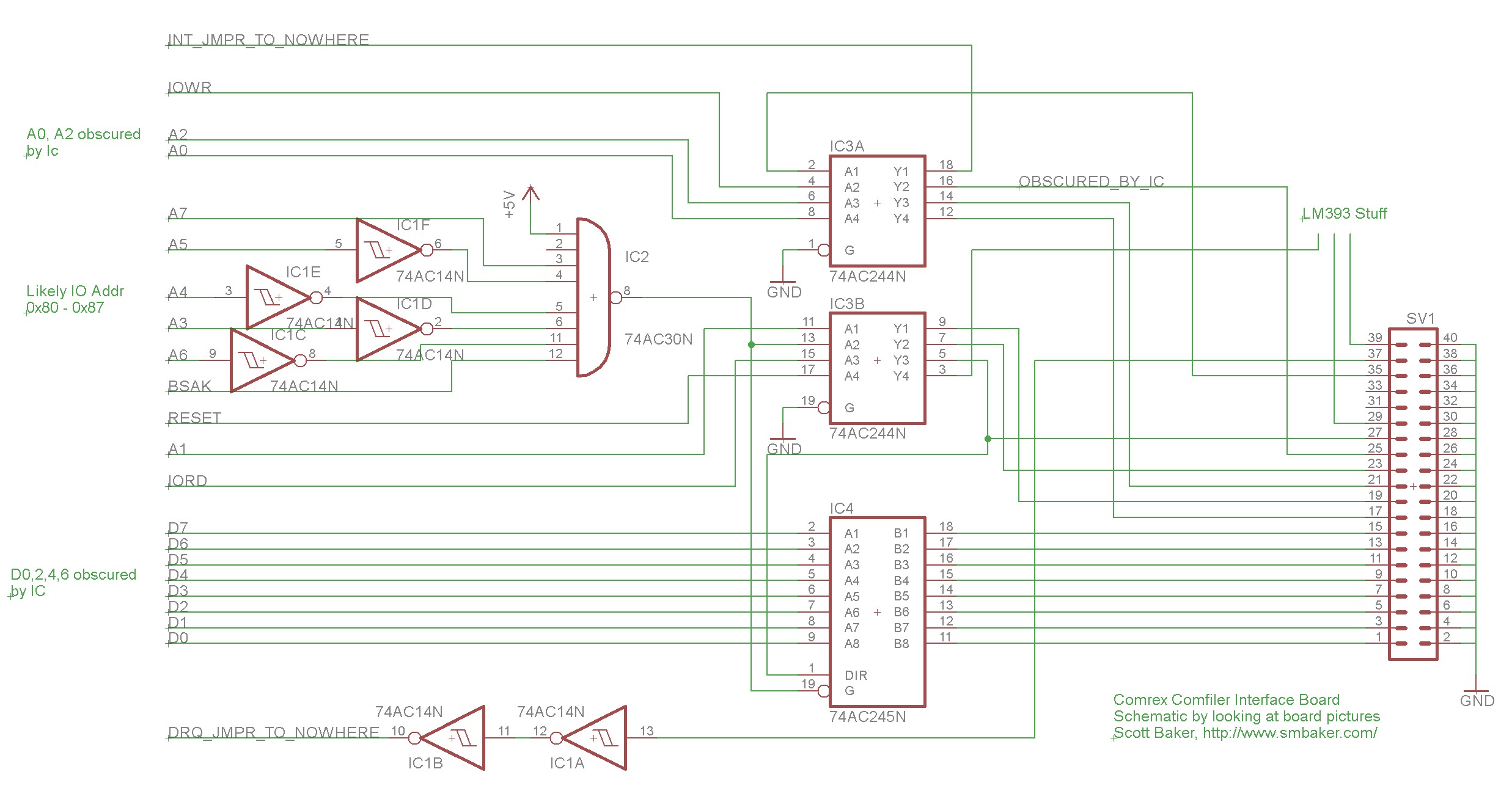
The Comrex Comfiler was an MFM hard drive for the QX-10. Few of these exist today, but DeltaDon at the VCF Forum was able to send me a couple pictures from the Comfiler’s controller board. From that I managed to reverse engineer approximately 80% of a schematic.
Coimrex Comfiler Hard Drive Controller Reverse-Engineered Schematic
The schematic is basically an address decoder, a data buffer, and an address/control buffer. The address decoder appears to decode addresses 0x80 to 0x87, which seems like a reasonable likely location to stick an MFM controller IC. The DRQ and INT lines did not appear to be wired through to the edge connector; maybe comrex build the board with the intention they could be jumpered for advanced use. There’s also an LM339 and some associated resistors and capacitors that I did not bother to map out on the schematic — my working theory is that this formed some sort of reset circuit, perhaps implementing some hysteresis. Several traces I had to take my best guess at as they passed under ICs; if I had an actual Comrex controller then I could do a better job.
Implementing compatible hardware and them patching the driver in the same way that Wayne and John did would be a solution that allowed the existing Epson BIOS to be used.
Another option, the uIDE-8
I found the uIDE-8 from some forum threads by user JonB over at VCF. A wiki page for the uIDE-8 is available at http://www.cpcwiki.eu/index.php/UIDE_Universal_IDE_adapter_cards_for_Z-80_computers. This is a general purpose solution that could be used with most Z80 computers. Compatible hardware would be straightforward to implement on the QX-10 expansion bus.
However, the uIDE-8 driver requires “MOVCPM.COM” to free up some space for the driver, and not all Epson CP/M distributions include the MOVCPM tool. So far I’ve only found one relatively old Epson CP/M release that includes it. I will keep looking for others.
To be continued
Next step is to make an Eagle package for the QX-10 expansion board, and then drop on an address decoder and some buffers.
In this post, I design sound and speech boards for the Epson QX-10 computer.
Purpose
I’ve been having fun with my Epson QX-10 — in the previous blog post I built a compactflash IDE storage device for it. But, the computer has four more expansion slots and I want to fill them out. I figured I’d start simple. The AY-3-8910 is a popular sound chip for Z80 based systems; I was last introduced at it when looking at Ed Brindley’s sound board for the RC2014. I knew it would be relatively simple to interface. The SP0256A-AL2 speech synthesis IC is also quite easy to work with, having designed boards to fit it to an RC-2014 and a PC myself. I’d have preferred to do a Votrax SC-01A board, but the votrax ICs are much less plentiful than the SP0256.
Sound Board
Below is the schematic for the sound board:
Epson QX-10 Sound Board Schematic
The sound chip is the venerable AY-3-8910. This thing is a little bit wonky in how the control signals work:
BDIR
BC2
BC1
AY-3-8910 Function
0
1
0
Inactive
0
1
1
Read from Sound chip
0
1
0
Write to Sound chip
1
1
1
Latch register address
I explored the typical mappings on the MSX and the ZX spectrum. The MSX-style addressing (ports A0 – A2) seemed most appropriate, but the QX-10 already has an option board that can be placed there. So I ended up putting my board at 0xD8. This lines up nicely with the default address on my IDE board, which is 0xD0.
Computer
Set Register
Write Data
Read Data
QX-10 Sound card (www.smbaker.com)
0xD8
0xD9
0xDA
MSX
0xA0
0xA1
0xA2
ZX Spectrum
0xFFFD
0xBFFD
0xBFFD
To perform this addressing, I used an ATF16V8B programmable logic device (PLD). PLDs are relatively period-accurate, and they allow you to implement several logic gates in a single IC. An advantage of the PLD is that it can be easily reprogrammed if a mistake is made. The PLD handles translating the address lines (A0-A7) the BSAK, read and write strobes, etc., and generates the BDIR, BC1, and CS signals. Find the pld files in the pld/sound directory in my github repo.
The CS signal together with the BDIR signal are used to select a bidirectional data buffer, because buffering the IO on the card is good practice.
Audio output is mixed together via a resistor mixing network and fed into an optional LM386 amplifier. You can use the LM386 to drive a speaker, or use the audio-out jack with an external speaker.
JP3 and JP5 are used to select the clock. I use JP3=1-2 and JP5=2-3 to select the QX-10’s internal clock, and to divide that clock by 2 to get a 2MHz clock to the AY-3-8910. You could choose to instead use an external oscillator by jumpering JP5=1-2.
Below is a picture of the completed sound board, with the default jumpers:
Epson QX-10 Sound Board
The board is a straightforward implementation of the schematic. As pictured above the optional crystal oscillator is not installed, and it is jumpered to use the QX-10’s clock, divided by 2. The dip switches should be set to off-off, or left uninstalled.
For playing sounds, I modified Wayne Warthen’s tune player that is included on the RomWBW distribution.
Speech Board
Below is the schematic for the speech board:
Epson QX-10 Speech Board Schematic
I went a little bit different route on the speech board than on the sound board. Rather than used a PLD, I used a good ol’ 74HCT688 magnitude comparator and a dip switch. Set the dip switches to off-off-on-off-off-off to place the speech board at its default address of 0xDC (right along side its friend, the sound board). A 74HCT32 is used to combine the CS out of the 74HCT688 with the IO Read (IOR) and IO Write (IOW) strobes from the QX-10. For writing, we trigger the ALD pin on the SP0256 to load a phoneme off the data bus. When reading, we use a 74HCT244 to put the STB and LRQ signals onto D0 and D1. This allows you to write a phoneme to 0xDC, and then loop reading 0xDC and wait for D1 to go low.
You should also be able to install a jumper on the INT pin, and have the speech synthesizer generate interrupts when it is ready for a new phoneme. I have not tried this.
As with the sound board, I used a LM386 as a mono amplifier. There are two low-pass filters straight out of the SP0256 data sheet. The data sheet calls them 5KHz filters, but my math does not add up. I’ll trust the datasheet knows what it’s talking about.
Below is a picture of the completed board:
Epson QX-10 Speech Synthesizer Board
Not much to see here — the two LED footprints were useless (not polled often enough to be “visible”), and will be removed in the next iteration.
pld/sound/sound.jed – binary version of PLD for the sound board. Burn it with a TL866 or similar EPROM programmer.
apps/sound.img – disk containing music player (tune.com) and several PT3 files. I couldn’t get the MYM files to play correctly, only the PT3 files. This disk is 16 sectors of 256 bytes each for the first two tracks and 10 sectors of 512 bytes each for the remaining tracks.
asm/tune.asm – my hacked-up variant of Wayne Warthen’s tune.com music player.
apps/speech.img – contains TALKER.BAS, a program for testing the speech synthesizer. As with the sound board, this image is 16 sectors of 256 bytes each for the first two tracks and 10 sectors of 512 bytes each for the remaining tracks.
This page is where I’m going to briefly collect all my Coco-2 thoughts. Starting with my videos on the subject,
Some history
The Coco-2 was the first computer I ever owned. Not necessarily the first one I ever used — that was either the IBM PC 5150, or the Convergent, or probably some 8-bit Atari in a department store. But the Coco-2 was the first one that earned a permanent place in my room. I remember bits and pieces of it. I had a speech synthesizer (took me a long, long time to figure out it was a RealTalker), I had a light pen, I had the single full-height floppy drive. I played Sands of Egypt and failed somewhere mid-way through. So I was excited to take on some Coco projects.
Buying a Coco
So you want to buy a Coco? Well you’re in luck, because they show up constantly on eBay. You have several versions to choose from, Coco-1, Coco-2, Coco-3, and even the MC-10 (which isn’t really a Coco). My first Coco was a 16KB extended basic Coco-2, so that’s what I set about buying. I had been watching eBay for years, and finally saw an auction for a NOS (new old stock) 16KB extended basic model, and the price wasn’t outrageous like the NOS ones often are, so I snatched it up. Watching the first video at the top of the page, you can see me unbox it.
Upgrading the memory
I remember back in the day upgrading the RAM on my Coco-2. I’m not sure if it was a 64KB or a 256KB upgrade, but I do recall plugging in some kind of piggyback ICs, and dealing with bank switching, so perhaps I had gone all the way to 256KB. Anyhow, my first modification to the NOS 16KB Coco was to boost its RAM from 16KB to 64KB. How you do this depends on which version of the Coco you have. In my case, it was simple enough to replace 8 DRAM chips with 4164s, and add a jumper in the appropriate place.
16KB Color Computer 2, Korean Manufactured, Upgrading to 64KB
Installing a CocoVGA Board
Next I decided I was going to add a CocoVGA board. While I had the motherboard out to do the RAM upgrade, I pulled the 6847 and installed a socket in its place. Having a socketed 6847 is a necessary prerequisite for the CocoVGA board.
Scoketing my 6847 in preparation for a CocoVGA board
Unfortunately, the wait list for the CocoVGA turned out to be kinda long, so this particular step is on-hold for now. I will update the blog when I my slot on the waitlist comes up.
Installing a composite mod
Given that I couldn’t get my hands on the CocoVGA board, I decided to go for the next-best thing, a high-quality composite modification. Ed Snider sells really nice composite boards on his website. Ed came up with this board when he came across a Coco2 that had a factory, yes a *factory*, composite output. These were apparently Cocos manufactured for educational purposes back in the day. Rather than using a TV, the educators used composite monitors. Installing Ed’s board is a little bit of desoldering work to get the RF modulator out.
Removing the RF Modulator from the Coco in preparation for a Composite Board
Next, the composite board is installed in it’s place, together with a few wires to supply power:
Composite Board from The Zippster Zone installed in my Coco-2
The video output was much improved. No more nasty ghosting. No more weird wavy lines. The Channel-3/Channel-4 switch is now a color/mono switch, and the mono output is really incredible. It is a color computer though, so most of the time you ought to operate it in … color.
Building a Multi-Pak Interface
One of the things I never owned back in the day was the MPI. The MPI allows you to select between four cartridges. You can either do so manually using a switch, or you can do so under software control. For devices that are merely peripherals, without a ROM, you can often operate them simultaneously together with a cartridge that does include a ROM, like the disk controller. This is really nice for using a speech synthesizer and a disk at the same time.
MPIs can be pricey, so I found some pcboard artwork from The Little Engineers, I built it, and I designed a 3D printed case around it.
MPI Board made from artwork by TheLittleEngineers3D Printed Case for TheLittleEngineers MPI Board
The board worked as expected. I was able to switch between ROMs, and I was able to simultaneously use the disk with some other cartridges, such as the speech/sound cartridge. I installed a big rotary knob instead of the little dip switches.
You’ll notice there’s a few weird things about the board, for example the slots are not equally spaced. They’re also number 4-to-1, rather than 1-to-4. I reworked the board a little and have a custom board on order to change it to my preferences.
The Speech/Sound Cartridge
I knew I had a speech synthesizer back in the day, and I wanted to get one again, so when a good deal on a Speech/Sound Program pak came up on eBay, I went ahead and ordered it. It was such a “good deal” because, as it turned out, the SP0256A-AL2 speech synthesizer IC was bad. It took me a while to diagnose that, and fortunately I had a spare SP0256A-AL2 on hand.
My speech/sound pak had a bad SP0256 in it
I also replaced a 10uF capacitor, just because it seemed like an easy culprit, and a failed SP0256 was about the last thing I considered. The speech/sound pak includes both a SP0256A-AL2 speech synthesizer and an AT-3-8913 sound chip. It can play pretty decent music, and it plays it right out the TV speakers. It’s a pretty well-engineered cartridge, featuring an additional micocontroller, several op-amps to ensure audio quality, etc.
Unfortunately, it wasn’t my speech synthesizer…
The Colorware Real Talker
I realized quickly that the speech/sound pak wasn’t the right one, so I set about digging out old Rainbow Magazines until I finally came across an ad for a Colorware Realtalker. I searched and searched and search and I finally found someone, Rod, who owned a Real Talker. He was kind enough to send me some pictures, and between his pictures and my looking at the Colorware software, it would have been enough for me to reverse engineer the thing. But then I decided owning the real thing would be even better, so I purchased it from him. Thanks again, Rod, that Real Talker cartridge is exactly what I remember. Almost… it turns out there are two versions, the Coco-1 version and the Coco-2 version. Rod’s was a Coco-1, powered by the Coco-1’s internal 12V supply, mine was a Coco-2 version, powered by an external wall-wart. It was close enough though, and probably the only one I’ll ever see again! Here are some pictures I took of the Real Talker:
Colorware Real-Talker pcboard, top viewColorware Real Talker, pcboard, bottom view
The design is pretty simple. There’s a bit of address decoding (74LS30 and 74LS27) to put the Votrax at the right address, a latch (74LS75) to latch the pitch bits, and a Votrax SC-01-A that’s tied directly to the data bus. While the Votrax is talking, a diode pulls down the HALT line on the CPU. The Coco literally can’t talk a chew gum (or do anything at all) at the same time. Below is my reverse-engineered schematic:
Colorware Real Talker Schematic. CAUTION: This is reverse-engineered and unverified
Note that the schematic is unverified. I am going to have a pcboard fabbed, and will try it out to make sure I got it right.
Also note that I ran into a couple of issues using this:
My Coco-2 doesn’t have +12V, and this is a Coco-1 version of the Real Talker. I plugged it into my homemade Multi-Pak interface to get the +12V supplied.
My homemade Multi-Pak apparently had a bug and wasn’t passing addresses above 0xFF7E on the bus. The Real Talker is at 0xFF82, and I spent hours trying to figure out why it wasn’t working, even resorting to desoldering the SC-01-A to make sure it was good. Eventually I found the problem with the homemade multi-Pak, and patched it to pass 0xFF82.
The audio sounded terrible. It turns out that the Real Talker’s audio output was at too high a voltage and was being clipped by the Coco-2’s audio amplifier. This might be a side-effect of the Coco-2 not having +12V internally. Hypothetically, the Coco-2 version of the Real Talker may include a resistor divider or pot to reduce the output level. I really wish I had a schematic to know for sure. Installed a pot between the Real Talker and the Coco-2 to reduce the audio level, and the output is now perfect.
Once I vet the board design, I’ll be sure to make it public so anyone can build a Real Talker… well, at least anyone who has a spare SC-01-A just laying around.
The Colorware software is really nice, it has a binary that adds “SAY” and “CONVERT” basic statements. The “SAY” statement does text-to-speech conversion. The “CONVERT” statement will perform text-to-speech on the source of the currently loaded basic program and replace it was a translated version that no longer requires the binary.
The CocoSDC Floppy Drive
Back in the day, I owned a single full-height floppy drive for my Coco-2. Unfortunately, I have no idea where my original disks with all of my original programs are. It would have been fun to see what my old software was like. I remember writing a disk directory sorter that worked perfectly … exactly once. The second time you ran my directory sorter, it scrambled the disk. Oops.
Anyhow, I wanted a floppy drive again because floppies are a whole lot more convenient than tapes. However, they’re still finnicky often troublesome devices forty years later. Floppy drives go out of alignment. 5.25″ disks are hard to source. You’re constantly using sneakernet to walk floppies between your windows PC and your vintage PC. Better to use a Gotek. Even better to use Darren Atkinson’s CocoSDC. Ed Snider sells CocoSDC on his website too.
CocoSDC does hardware emulation of the floppy drive controller, so it works with just about anything. You store your disk images in a set of files on a SD-Card. The Disk OS includes handy commands for mounting directories. It even features flash memory and can be flashed in-place to load custom ROM images. I can’t recommend the CocoSDC enough — it’s really convenient.
I still want one of those old full-height floppy drives though, and I’m sure I’ll probably end up with one.
Resources
My Github Repo of Coco Stuff at https://github.com/sbelectronics/coco. Here you will find a dumping ground of my coco-2 related stuff. The schematic for the Real Talker is there. The STL files for the 3D printed case for the TLE MPI is there. Enjoy… and use at your own risk.
In this post, I prove a broken clock can be right more than twice a day:
Background
The Heathkit GC-1000 Most Accurate Clock is a timepiece from 1983 that receives time broadcasts on the WWV or WWVH stations operated by the US Government. These stations are received at 5MHz, 10MHz, or 15MHz. The clock is capable of automatically scanning all three of these frequencies, or you can lock it to a specific frequency.
These signals are broadcast from Colorado and Hawaii. How well you receive these signals depends on everything from local interference to sun spots and atmospheric behavior. 15MHz is most active during the day. 5MHz is most active during the night. 10MHz is most active during the transitions between night and day. Here in Oregon, I typically receive the Colorado broadcast, though I’ve been known to occasionally pick up the Hawaii broadcast, or even to pick up both broadcasts at the same time.
These broadcast, over the course of approximately 40 seconds encodes a series of bits that tell the current time and date. There’s also a man (for Colorado) and a woman (for Hawaii) that will recite the next time timestamp near the end of each minute interval. The time is encoded using a series of 1000Hz and 100Hz tones.
The GC-1000 continuously attempts to receive these WWV (or WWVH) signals and uses the timestamp not only to set itself to the current time, but to also trim its internal oscillator so that the accuracy of the clock between syncs improves over time.
The Clock Purchase
I found a broken clock on eBay and purchased it.
The seller’s listing described the clock as “powers on, lights up, but then nothing happens” and “missing some screws”. Never having owned one of these clocks before, I assumed it was indeed broken, but having better than average diagnostic skills, I figured I stood a good chance of being able to fix it.
First, a GC-1000 that doesn’t show any digits is not necessarily a problem. The clock does not display the time until it was synced with WWV. It can sit like this for four minutes, four hours, four days, or for-ever. To make the clock display the time, you have to give it a strong WWV signal (perhaps even from an external antenna). It has to receive an accurate time signal from WWV two (or three?) times in a row before it will sync the time. This can be a bigger hurdle than you might give it credit for.
Diagnosis
I tore the clock apart. It was not only missing some screws, but the plastic standoffs that mounted the top shell of the clock to the bottom had broken and been previously discarded. The top and bottom shells had evidence of some velcro remnants, so it seems to previous owner had been holding it together with velcro. Connectors to the RF board had been left disconnected. The potentiometers on the tone board showed evidence they had been fussed with.
The GC-1000 has an internal switch that will place it into diagnostic mode. The manual for the GC-1000 tells you exactly what to do. I flipped the switch and the display flashed erratically between lighting all digits and lighting nothing. It kept flicking on and off randomly. Sometimes it would respond to the diagnostic pushbutton and sometimes it would not. Once it displayed “1000 2” but then it flickered back off as soon as it had displayed it.
I tore down the part (watch the video and you’ll see a similar teardown). I removed all boards. The bottoms of the boards had a black goo residue, some remnant of the flux. I could see that it had either been recapped, or the original build had gone awry and damage had been repaired. The damage was around C212, a capacitor, and U202, a 5V regulator. Putting the board under the scope, I was able to determine that although a previous owner had attempted to replace C212 and repair the traces, he/she had not repaired the trace from the microcontroller to C212. This trace is the microprocessor’s reset line.
And just like that, the problem was solved and fixed. The damaged trace had left the microcontroller’s reset line floating, and because of this it was suffering from spurious resets. I scrubbed off the black goo with alcohol and a toothbrush. I replaced all the caps on the main board (while it’s out, might as well give it a thorough recapping), and I reassembled the clock.
Now the diagnostic mode worked, and I was able to adjust the tone board for 1000Hz and 100Hz tone matches according to the manual.
I spent some time fussing with it, trying to get it to sync, eventually gave up, and sat down at the computer to do some work.
First Sync
Some hours later I stretched, looked around the office, and exclaimed “<expletive>! The clock is displaying a time! <explective>!!!”.
A watched clock never syncs. The key is to not give the thing any attention, and it will surprise you.
At this point, I started shooting parts of the youtube video, to show the functioning clock. I also moved it over to its permanent display location, and I cleaned up the antenna wiring.
Last sync
Moving the clock seemed to doom my success. Over the next two weeks, it would occasionally, rarely, sync. If I unplugged it and plugged it back in, it might sync or it might go days before syncing again.
I became increasing frustrated and started spending time and money on antennas
First Antenna: Internal Random Wire
My first antenna was a random wire along the ceiling in my office. Being inside the office, it did not require me to go outside and run wires, nor did it lead to any unsightly “ham radio antennas” sticking out of the home that someone could complain about. The indoor random wire seemed to often pick up strong signals, but the clock still would not often sync.
Second Antenna: External Random Wire with a 9:1 Unun
For the second antenna, I figured I would run an inconspicuous external random wire. I also built a 9:1 unun, because that’s what the Internet said I needed.
The second antenna didn’t work much better than the first. Maybe a little. Not much.
Third Antenna: The Youloop
Doing my online research, I stumbled across the youloop, a simple loop antenna, and I ordered a youloop clone from Amazon. I did this without realizing that a youloop is best suited for sensitive SDR radios and not necessarily the best choice for my 1983 heathkit special.
The youloop seemed to work altright. Maybe a little better than the random wire antennas. Or it might have just been wishful thinking
Fourth Antenna: The MLA-30+ MegaLoop
In parallel with ordering the youloop, I also ordered an MLA-30+. This is another loop antenna, but it’s one that includes a built in amplifier, right at the antenna itself. The MLA-30+ performed better than any other antenna I have tried to date. Whereas previous antennas were incapable of tuning the 5MHz band on the radio, this one did indeed pick it up. It also seemed to tune the 10MHz and 15MHz louder than the other antennas. This isn’t surprising, the inline amplifier seems to help a bit.
The GC-1000 Enigma Clock still would not reliably sync the time.
Recapping, Cleaning, and Fixing Things
In parallel with all of the antenna drama, I was little by little trying to replace or improve parts of the clock. Here’s a log of every single change I can remember making:
Replace electrolytics on the main board. This step I did as part of the original repair.
Repair the broken trace on the main board.
Replace the wiring to the DC jack, which had previously deteriorated and separated.
Replace the wiring to the RS232 DB25. It was frayed and about to fall apart.
Spray deoxit in the slide switches for debug mode and for display on/off. These are poor quality switches and should really be replaced. Even after hitting them with the deoxit, they’re still finnicky.
Replace R434 and R444 on the tone decoder board with 25-turn potentiometers. First I wasted my time and used random China Ebay potentiometers. Then I came to my sense and installed name-brand Bourns pots from mouser. If you care about the accuracy of your pots, and if you care to not have them drift, but the name brand ones.
Replace electrolytics on the tone decoder board. This included replacing C422, a 3.3uF electrolytic with an 0.33uF film capacitor. The manual says 0.33uF, but I found 3.3uF on the board. The incorrect part may have been part of a previous owners recapping, or it may be the documentation is wrong and that is the cap Heath actually supplied.
Clean all board-to-board connectors. The pins you can clean with a pencil eraser. I also sprayed some deoxit inside the female housings.
Reseat every single IC in the clock. The IC sockets are very poor quality.
Replace electrolytics C354, C353, C355, C357, and C301 on the receiver board. These parts you can probably replace without throwing the RF alignment completely out of wack.
Replace IC sockets for the LM567 tone decoders and the LM3900 op-amp on the tone board with machine-tooled pin sockets.
Replace the LM567 tone decoders and the LM3900 on the tone board with new nichicon caps from Mouser.
Does it work now??
Right after replacing electrolytics on the RF board, and replacing the LM567 and LM3900 on the tone board, and performing yet-another-tone-board adjustment, the enigma clock immediately (while I wasn’t watching it, of course) synced with WWV, and as I write this paragraph of the blog post on a lazy Sunday afternoon, the enigma clock has been in hi-spec for a continuous two hours. It’s a new record.
In this post, I add a panadapter to my Drake R-4B.
Background
In late 2021, I decided to become a Ham Radio operator. This involved passing a couple of tests — my technician and my general exam. It took a little bit of study, and soon being an amateur radio operator was within my grasp! I just needed a radio. As people familiar with my blog already know, I’m fond of vintage electronics, and I’ve done a couple tube projects in the past. So, I decided to buy a couple of “Drake Twins” on eBay.
“Drake Twins” typically refer to a pair of radios, a transmitter and a receiver. These can be operated separately, or they can be slaved together so the receiver can set the frequency of the transmitter and vice-versa. I purchased an R-4B and a T-4XC. Turns out I underestimated the amount of effort needed to repair the old rusty R-4B, so I ended up purchasing a second R-4B. Oops. Well the second one was in considerably better condition than the other.
Anyhow, restoring/repairing the radios is probably the subject of another blog post, so suffice it to say I managed to get them working. However, I found it hard to find folks to talk to. Maybe it’s my newness and lack of experience, or maybe it’s my lower-than-usual antenna, or maybe it’s poor band conditions, but would spend a lot of time searching for signals. This led me to jump into this panadapter project.
What is a “panadapter” ?
A panadapter takes a radio that is normally designed to operate within a limited bandwidth, typically 4KHz for AM , 2.4KHz for SSB, or 1.2KHz for CW, and adopts that radio to output a wideband signal. This wideband signal could be viewed with a spectrum analyzer or a software defined radio (SDR). The wideband signal allows you to “see the whole band”. The etymology of the prefix “pan-” may trace back to Greek, and generally means “all”. For example, “pandemic” is a disease occurring worldwide. Well, a “panadapter” is an adapts a radio signal to be band-wide. It could even be wider than just a single band.
So what’s the value of this wide-band signal? Well, by seeing the entire band at once, you can easily see everything that’s going on. You can see 2.4KHz SSB transmission, you can see 400KHz CW pulses, or you can see wide AM transmission.
Panadapter Display using the Popular SDR Console Software
In the above display, the signal I’m tuned to is right in the middle, beneath the narrow green bar. That’s a 2.5KHz SSB transmission. To the left of it, you can see several more 2.4KHz SSD signals. On the right side, you can see many thin lines that might be CW or other digital signals. Interference/noise is also shown on the display, so you might see some wide wobbly noise signals.
The “waterfall display” continuously runs, with new data appearing at the top, flowing down the screen. My wife thought it looked like “The Matrix”. Well, sort of, not really. Anyhow, notice the two very strong pulses to the left of where I’m tuned — those brief signals could have been someone calling “cq cq cq” looking for a contact. Just spinning the dial through the band, you might well miss them. But the panadapter lets you see the whole band at a glance.
How do we make a panadapter?
First we need to understand a little bit about our ham radio. Our Drake is a double super heterodyne receiver. It takes the incoming RF and it mixes it with a desired frequency from a local oscillator, to center that frequency around an intermediate frequency (IF). In our case, this IF is 5645 Kilohertz. The reason this is done is because it’s easier to design filters and amplifiers around a fixed frequency than to design them around broadband. So it filters this 5645 KHz, and then it mixes it again down to 50 KHz, where it can filter and amplify it some more, and then finally a detector can covert it to audio. To make our panadapter, we need to intercept the signal right after the first mixer stage.
Panadapter added to a Tube Ham Radio
As you can see, we’ve added some additional components. The original radio pipeline is in blue. We’ve added some parts in green. These parts are a buffer, because we don’t want to overly load down the RF signal within the receiver, and a Software Defined Radio (SDR) dongle. Finally, we display the spectrum on our Windows, Mac, Linux, or other PC. You might be able to use something like a TinySA spectrum analyzer too.
The SDR Dongle needs to be able to handle the intermediate frequency from your radio. My Drake has a 5645 KHz intermediate frequency, but your radio may differ. Some radios have 9 MHz. Some radios have 455 KHz. Some radios have something else. Not all radios can tune these frequencies. For example, my rtl-sdr dongle does not. I have a “HackRF One” Dongle that does handle it. So choose your SDR wisely.
It’s important to notice that the frequency your SDR receiver will be centered around the IF. If you tune 7.238 MHz on the receiver, the SDR sees the IF (5645 KHz in my example). If you tune 28.5 MHz, the SDR sees the IF. As you tune your radio left or right, the spectrum is going to move to the left or right. Your tuning point will always be right in the middle of the display.
Building a buffer board
Now let’s talk about the buffer board. Here’s where life becomes a little difficult dealing with an old tube radio like the Drake. Tube radios are often high impedance signals. They’re meant to drive loads into the hundreds of kiloohms or even into the megaohms. If you take a regular garden variety amplifier designed for a 50 Ohm input impedance, you’ll suck the signal right out of your radio and there will be nothing. You’ll completely load down the receiver.
When I started this project, I originally tried Clifton Laboratories Z10000 Buffer from DX Engineering. I connected it to my 1st Mixer as above, and it rendered the receiver pretty much mute, because it drained all the signal. There was some speculation that an appropriate coupling capacitor might help, but really that amplifier board is not designed for a high-impedance input. It’s designed for modern solid state radios with a low impedance.
I asked for some tips in the Drake mailing list and was advised to use a high impedance FET Source Follower. I ended up using the following design:
FET Buffer from Drake T-4XC Schematic
This doesn’t look like one of my own schematics, and that’s because it isn’t. I lifted this circuit right out of the carrier oscillator circuit from my Drake manual. The T-4XC’s carrier oscillator uses a 2N2953 for the oscillator and then buffers it using a pair of 2N2950 transistors. I grabbed one of the transistor stage schematics. The circuit is fairly simple. The incoming RF from the 1st Mixer is coupled by a 10pF capacitor. Then it goes through a bias resistor network, then it’s buffered by the 2N2950 JFET. The JFET’s “Drain” is connected via a 100ohm resistor to +12V, and the “Source” drives a 470ohm resistor to ground. We couple that out to the SDR through another capacitor (“C” in the above diagram, 0.001uF in my prototype)
I built that circuit using some proto-board and stuffed it into the drake.
Prototype Panadapter Buffer
The single red wire is my input to the board from the receiver. I probably should have used shielded cable, but it’s short, and it didn’t seem to cause much trouble. The two 2-pin dupont plugs are for power (yellow) and signal out (green).
Prototype Installation
The board needs approximately +12V for operation. I got this by installing a diode and capacitor on the R-4B’s 12.6VAC filament supply. This forms a half-wave rectifier that will have somewhere around 14V to 18V on it, depending on the load. It’s not perfect, but it worked. Then I installed the board need V2, the first mixer. I connected it to V2 pin 5, and rand a cable out the back to an SMA connector:
Panadapter installed in Drake R-4B Receiver
My S-Meter does read low since adding the panadapter board. I do plan on experimenting a little more to understand this. It didn’t suck all of the signal outlike the Z10000 board did — the radio actually sounds really good after adding my FET Follower Buffer, it’s just that the S-Meter reads low. It’s entirely possible that I just need to retune the S-Meter sensitivity and offset. One really needs to do a realignment of the whole stage after altering the properties of the RF circuit.
Other Concerns
I had to install a hefty RF choke on the cable going to the SDR, or it would lock up whenever I transmit. It’s not the signal that was causing the SDR to be overwhelmed, I think it was stray RF on the coaxial cable. I use an end fed half wave (EFHW) antenna, and it throws some RF about.
In this blog post, I build a raspberry pi based DDS VFO for my Drake Ham Radio
Purpose
My Drake R-4C/T-4XC Amateur (Ham) Radio has been a lot of fun, but it can also be a lot of work keeping it on frequency. The mechanical nature of the VFO/PTO assembly I think lends itself to frequent drift as temperatures shift, or as the voltage inside the receiver changes. In addition to being hard to keep on frequency, it’s also hard to dial into a desired frequency, as very tiny movements of the dial are necessary. Especially when you’re using digital modes, like FT8 (and yes, I do FT8 on the old tube Drake), you want the frequency to remain constant.
One solution is to use a digitally synthesized frequency to drive the radios rather than their internal variable oscillators. Modern ICs can put out a pretty stable digital frequency. No more drift, and easy to dial in to exactly what you want.
Drake Basics
There is an injection line that connects the Drake twin receiver and transmitter. This injection line can be used in either of two ways, Receiver -> Transmitter (RVCR Mode), or Transmitter -> Receiver (XMTR Mode). It can also be ignored entirely (SEPARATE Mode). This line carries your desired frequency plus 5645 KHz. For example, if you want to tune 7.074 MHz, then the INJ line will be at 12,719,000 Hz. If you want to tune 29.5 MHz, then it’s at 35,145,000 Hz.
Tuning the transmitter is easy; the transmitter will happily accept an AC waveform at its INJ connector so long as the transmitter is in RCVR mode.
Tuning the receiver is a little more tricky. It outputs on the INJ line, unless it see a DC signal in the neighborhood of about -27V (it’s still an oscillating waveform, it just has a big negative DC offset applied to it). This is what happens when you put your transmitter in XMTR mode. However, there’s an additional way to pull this off — if you switch the receiver to an unused crystal socket, the local oscillator will not oscillate, and it’ll happily pick up whatever AC waveform you supply on the INJ port, even without the big negative DC offset.
So the first approach would be to stick a Tee on the INJ line, switch the receiver to an unused crystal, and then put our digitally synthesized waveform onto that INJ line. This works, sort of.
Drake Injection using a Tee
The problem with this approach is that the receiver tends to attenuate the injection signal, especially if you are either poorly aligned, or if you don’t have the preselector set right — there are coupling capacitors tuned to the preselector knob position. Remember, the Twins were not really designed for a signal to be injected to both of them this way. The attenuated signal then does a poor job of driving the transmitter, and I saw low output power.
For that reason, in this article, I will show a DDS-VFO with two drivers, so we can cut the injection cable, and drive the Transmitter and Receiver separately:
Drake injection using two drivers and independent injection cables
DDS ICs
There’s lots of choices these days for the DDS IC. I went with an AD9850, which is the same IC that K3JLS uses in his DDS-VFO for the TR7. This IC is cheap and there are carrier boards readily available on ebay and on ali express:
AD9850 module on aliexpress
Twelve bucks may be cheaper than you can buy just the components yourself, and it’s certainly cheaper than you could assemble the thing yourself. Sometimes these premade modules can be a deal.
Schematic
The schematic is shown below:
Raspberry Pi DDS-VFO for Drake Twins (R-4C, T-4XC) Schematic
The upper left is a raspberry pi, connected in the traditional way. The lower left is an atmega328, just in case you’re the type of person that a raspberry pi is not for you. The lower right section is where it gets interesting.
The DDSVFO is driven by four lines — clk, load, data, and reset. It works like a shift register. You clock in your data and then hit the load line to load the data and make it active. The DDS-VFO outputs a waveform that we couple with a capacitor and then send to an optional butterworth filter. The butterworth filter came from K3JLS’s design, and as shown is not appropriate for this application because it has a 7 MHz rolloff, and we actually need a ~ 35 MHz rolloff. So just wire it across for now. I’ll come back to this and experiment with appropriate component values some day in the future.
After the butterworth filter (which you’ll just wire straight across, right?), there are a pair of output drivers. Each one uses a 10K pot for level control and then a two transistor driver using 2N2222 transistors. The buffer came from K3JLS as well, but I think it’s also the same circuit used by AA8V and W8DIZ.
I power the AD9850 module with 3.3V. There’s two options for this, either the 3.3V output from the pi, or an onboard 3.3V regulator using an LM1117-3.3. Using the pi’s regulator save a few parts, but you will hear artifacts from the pi on your receiver — if the pi executes a power-intensive operation, such as executing a command when you type it at the SSH prompt, you’ll hear a tick or snap on the audio. For that reason, I recommend using the separate dedicated 3.3V supply.
The 7812 regulator is option. If you plan to power this with 12V, then just wire the 12V regulator across.
The mute input can be used to implement separate transmit and receive frequencies. When the T-4XC goes to transmit, it’ll ground the mute line. We could detect this, and switch frequencies. I don’t implement that, yet.
All that remains is a bunch of headers for SPI and I2C peripherals, and the rotary encoder. I used a bourns optical encoder with 128 steps per revolution. You want a high-quality optical encoder like that, not a cheap low-step mechanical encoder. Find something cheap on eBay. I used 1K protection resistors on this, as I powered the encoder from 5V, and the pi is a 3.3V device.
Implementation
A picture of the completed prototype is shown below
On the left is my rotary encoder and keypad. The keypad uses cherry MX blue keyswitches. Pay no attention to the legends on the keycaps, I used spares from other projects. I’ll probably have WASD Keyboard print me up some custom keycaps once I’ve decided on all the functions.
On the right is the DDS-VFO unit. You can see a pi zero w upside down on the right, and the DDS module to the left. On the back are two SMA jacks, to which I’ve attached BNC-to-SMA adapters. Directly below the SMA jacks are the transistor buffers. One output section to the TX, and one output section to the RX.
On the front are two quad alphanumeric display units. Adafruit sells these boards, though in this case I respun their board to make it easier to daisy-chain. They’re controlled via I2C.
In this blog post, I create a new calibrator and a new amplifier for my Drake R-4C ham radio receiver.
Background
I’m relatively fond of these old drake tube ham radios, and I decided to upgrade my R-4B to an R-4C.
Note: many people don’t consider the R-4C to be an upgrade to the R-4B. While it came later chronologically, and included some modern technology such as a few transistors and crystal filters, it also moved much of the functionality to paid add-on modules, and it introduced an energy wasting / heat spewing amplifier stage.
Anyhow, the R-4C that I purchased came complete devoid of any options. It was utterly and completely stock. This blog post will chronicle some of my steps in upgrading the R-4C. I will mostly stick with doing period-accurate upgrades, what people would have done back in the day.
Crystal Calibrator
The crystal calibrator was an option that plugged into a four-pin socket in the R-4C. It produced a tone every 25 KHz on the band and could be used to accurately align your receiver to a particular frequency. It used a 100 KHz crystal, together with a capacitor to tune the oscillator exactly on frequency. The oscillator was divided in two and then divided in two once again, using a 7473 flip-flop IC. The schematic of the calibrator, reproduced from the R-4C manual, is shown below:
Drake R-4C Calibrator schematic, reproduced from R-4C Manul
It is critical that you use a SN7473N and not a 74LS73 or 74HCT73. When I tried the newer logic families they did not work, producing spurious triggers leading to erratic behavior. I tried to add a LED, but it did not work out properly — I expected the LED to be unlit when the calibrator was off, but there was enough leakage to dimly light it. Leave the LED out.
The board I built is shown below. Note that the red trimmer pictured below should probably be green rather than red. Red is 0-20pF and green is 0-30pF in the typical assortments. Also note that the picture shows a 1000pF monolithic ceramic capacitor for C182. This should be a 1000pF silver mica cap instead.
Drake R-4C Calibrator Board, Top Note: Use *green* trimmer cap, not *red* trimmer cap. Note2: Use a Silver Mica Film cap for C182, not a monolithic ceramic
The socket pins are 12ga copper wire, from my local hardware store. Note the additional bypass capacitor on the bottom; I’m not sure this was necessary — I added it while trying to diagnose a problem.
Drake R-4C calibrator Board, bottom
Below is a picture of the calibrator mounted in my drake:
Amplifier Modification
The R-4C amplifier is an inefficient design that dissipates a ton of heat. The heat is dissipated from the power transistor in the picture above right next to my calibrator board. It’s also right next to the VFO, and heat near the VFO can lead to drift. It’s surprising that Drake use this amplifier design when alternatives were available.
In 1979 Bob Sherwood published the design for a replacement amplifier based on the popular LM383T amplifier IC. I’m not going to discuss the design, as Sherwood’s article will do a better job than I ever could. Below is a schematic based on that article:
Sherwood-style R-4C Amplifier modification
I produced a board and installed it in my Drake R-4C:
Amplifier board installed in Drake R-4C Ham Radio
Sherwood’s article has a couple of cautions. First, that the length of the leads on the 1uF capacitor are exactly 3/4″ long. I found that this didn’t matter. Second, that the board is only grounded via the ground wire to the audio pot and not grounded to the chassis. I found this didn’t matter either; my board is grounded via a little metal L-bracket.
When I do revise this board, I’ll probably add an option to isolate the L-bracker from the ground.
I have a heat sink glued using thermal adhesive to the LM383. I don’t know whether or not this is necessary.
The only problem I ran into was when I accidentally installed a 2.7K resistor instead of the 2.7 ohm resistor. This caused low volume, high heat generation (200+ degrees F), hum, and probably a host of other problems. Make sure you get the component selection correct.
In this video I build a Z8000 (aka Z-8000) computer.
Background
I stumbled across the Z8000 on eBay one day and decided I had to go off and build myself a Z8000 single board computer. I couldn’t fit it all on one board, so I figured I’d made it a two-board computer, then I figured why not add some displays and it because a 3-board computer. Well, next month it’ll probably be a 5-board computer!
Anyhow, the Z8000 was conceived by Zilog back in 1979. It was a 16-bit microprocessor, intended to compute in the 16-bit microcomputer market. It’s contemporaries in the 80s would have been the 8086/8088 and the Motorola 68000. The Z-8000 didn’t quite make it, it was only used in a very few computers. x86 won out, Z-8000 lost.
Modular Design
The project is designed into a series of separate modules, with the intention that they could be mixed and matched, and the boards small enough that they can be manufactured at a reasonable cost. A 68-bin BUS connects the boards together, mostly exposing a 16-bit data bus, 20-bit address bus, and some selects for ROM and RAM. The boards are as follows:
CPU Board. Holds the CPU, Clock, address and data buffers, and bus and memory selection logic.
Memory and Serial Board. 1 MB of Flash, 1 MB of RAM, and two serial ports using a Z8530 SCC.
Display Board. Eight TIL311 displays for debugging info, with some provision for input switches and buttons
Schematics
TODO: Schematics of the CPU Board
The CPU board uses 74F373 octal latches to latch addresses off the AD bus onto the A bus. The latch occurs on the edge of AS, and an inverter is used to get the appropriate edge. 74F245 transceivers are used for the data bus. The data bus can be live all the time, but it needs to have the direct set appropriately, and this is handled by the TX/~RX pin to the the 245s, which comes from the PLD devices.
The Memory PLD is an ATF22V10C programmable logic device that is used to do memory addressing. See my github repo for the PLD listing. This handles decoding of the segment registers, together with the state pins, and the Byte/Word control line to select the appropriate RAM/ROM ics and to set the upper address bits (A16-A19). Using a PLD allows the segments to be easily reconfigured by the designer, and implement exotic schemes such as separate instruction and data segments. The PLD makes a number of segments available and the listing will indicate which is which.
The Bus PLD is another ATF22V10C. It’s job is primarily to decode the signals necessary to generate IOR, IOW (IO read and Write), and MEMR, MEMW (Memory Read and Write). Again, the PLD listing will explain exactly how this is done. It also generates a few chip selects for common peripherals.
Boot is handled using a flip-flop scheme borrowed from the Olivetti M20. When reset, the Z8000 will read the following:
FCW from address 00:0002
Segment from address 00:0004
Offset from address 00:0006
Then it’ll jump to that segment:offset and begin executing. The boot flip-flop on reset will assert a BOOT signal. The Memory PLD when BOOT is asserted will map the last bank (0x1F) of the Flash into segment 0. This causes the initialization vector to be read from Flash. As soon as A3 becomes positive, the flipflop will deassert the BOOT signal and memory addressing returns to normal (RAM at Segment 0). It’s entirely possible that a simpler scheme could be used, for example leaving the Flash at segment 0 and telling CP/M to use segments other than 0. However, the Olivetti approach seemed elegant and flexible.
A MAX811 IC may optionally be added to handle power-on reset. Without the MAX811, the CPU will sit there like a lump of coal until someone manually presses the rest button.
TODO: Schematic of Memory Board
The memory board uses two AS6C4008 SRAM chips for RAM, and two 39SF040 Flash memories for ROM. These are split into low (D0-D7) and high (D8-D15) on the data bus as appropriate. The RAM and ROM are selected by select lines that come from the CPU board.
Also on this board is a Z8530 SCC for serial IO. The SCC is wired to a pair of 6-pin headers than can be used with typical FTDI USB-to-TTL cables. A MAX202 is optionally provided to enable a physical DB-9 serial port for the RS-232 purists out there.
TODO: Schematic of Display Board
The display board uses TIL311 displays. These displays each take a 4-bit value and display a single hex digit. Eight displays allow four bytes to be displayed. The display board can be jumpered to display either the ports (SIO, PIO, or IDE) from the CPU board, or they can use a custom port selected by dip switches on a 74HCT688., In my configuration, I set the dip switches to place the display board at ports 0x50 – 0x53.
The display board also includes an input transciever than can allow a bank of dipswitches to be read by a user program. It’s my intention to use those dip switches to enable the bootloader to boot different functions. Four Cherry MX footprints are wired in parallel with four of the dip switches to enable momentary buttons. The input logic is optional, and I have not implemented it in the original video.
Implementation
TODO: Pictures of PCBoards
Note that 68-pin headers are either not readily available or prohibitively expensive. If you’re building the clover configuration like I did, just use 80-pin right-angle headers and sockets and cut them down to size. Yes, even the sockets can easily be cut to size with a pair of flush cutters. If you’re building the stacking configuration, then I’d suggest using 40-pin raspberry pi stacking headers, and cut one down to make it fit the 68-pins.
Boot Sequence
The boot sequence is as follows:
BOOT is asserted by the flip-flop. The Memory PLD maps segment 0 to Flash page 1F and segment 60 to Flash page 1F.
The loader’s initialization vector causes the CPU to jump to 60:0008.
Shortly thereafter, A3 becomes positive, and the boot flip-flop deasserts the BOOT signal. The Memory PLD now maps Segment 0 to RAM page 0. Segment 60 remains mapped to Flash page 1F.
The loader copies approximately 32KB from 60:0200 to 00:0000. This 32KB contains 4sun5bu’s z8kmon program.
The loader jumps to 00:0008., starting z8kmon.
Z8kmon displays a prompt over serial.
The user presses “B” to boot from flash. z8kmon copies 32KB from Flash page 0, to 03:0000 and then jumps to 03:0000. This 32KB is the start of the flash disk image, and the first thing in the image is the CP/M system code.
CP/M begins.
CP/M-8000 Notes
CP/M 1.1 is used. 4sun5bu in his github page includes a BIOS that supports IDE and the SCC. I modified this BIOS to use a Flash-based disk. At some point I’ll re-enable the IDE support, and maybe add floppy support.
TODO: IMPORTANT NOTE: Need to update the memtbl to use my segments instead of 4sun5bu’s segmentation scheme. The I/D segments are probably currently wrong.
Hunting the Wumpus!
If you watched the video, you might have noticed that I had some bugs where ED.Z8K and some other tools wouldn’t run. Those turned out to be a problem with memory segmentation for split I-D spaces, which I fixed. Then I managed to find some olivetti disks with wump.z8k on them… and now we have playing games on the Z-8000.
Z8001 Machine Code Monitor Ver.0.3.0
 Modified by Scott Baker (smbaker@smbaker.com) for Scott's Z-8000 Computer
 Press 'B' to boot or 'H' for help
   b
   Boot CP/M from Flash… Jumping to CP/M start
 CP/M-8000 BIOS ver.0.11.smbaker1
  CP/M-8000(tm) Version 1.1 12/19/84
  Copyright (c) 1984, Digital Research Inc.
 A>wump
 Instructions? (y-n) n
 You are in room 19
 Bats nearby
 There are tunnels to 2 16 18
 Move or shoot (m-s) s
 Give list of rooms terminated by 0
 2 16 18 0
 You are in room 19
 Bats nearby
 There are tunnels to 2 16 18
 Move or shoot (m-s)
Scott’s fork of 4sun5bu’s project. This has the bootloader, cp/m distribution, etc. I’ve forked it and modified the original to support using the 39SF040 as a flash disk.
In this blog post, I examine “The Trump Card”, a Zilog Z8000 coprocessor card that I bought on ebay:
A request for help!
I’m looking for the software that goes with this card. If you have this software, please get in touch. If at one point you owned one of these cards, or you were one of the people who implemented it, or you worked for Sweet Micro Systems, who sold cards commercially, then please get in touch. There’s enough information on the hardware that the card could in theory be reproduced, but the software is not known to be available. Without software, the card cannot be used, at least not as originally envisioned. You can reach me by leaving a comment on this page.
Background
The Trump card appeared in a pair of BYTE Magazine articles by Steve Ciarcia, back in 1984. These articles described a 16-bit coprocessor card for the IBM PC, featuring a Zilog Z-8000 microprocessor, together with 512KB of memory and a small boot ROM to boot the card. This enabled the following features:
TBASIC, a basic compiler that is mostly compatible with Microsoft’s BASICA.
C Compiler
Y multilevel-language compiler. This is described as being a structured assembler
Various debuggers, editors, and other useful utility programs
A CP/M-80 emulator
In addition to these executable programs that could be run on the card, there was also the ability to use the card’s RAM as a ramdisk in the host PC, for regular PC programs.
Building your own Trump Card
The Ciarcia article contains the schematics necessary for you to build your own Trump card. Ciarcia, being an excellent technical writer, takes you through the theory and operation of the card. It would be a relatively straightforward effort to build the hardware in modern times, probably with a few conveniences such as substituting a large static RAM for the 32 DRAM ICs, and replacing a plethora of 74XX logic with PLDs. We could probably get it down to a 2/3 length ISA card or if one really worked hard, maybe even a half length ISA card.
Once you built the card, the article instructs you to send a picture of your constructed Trump Card, along with $30 to Steve Ciarcia, and Steve would then send you the documentation and the software. It’s unclear how many people built their own Trump Cards. It would be a daunting task for a hobbyist to construct this large of a card back in 1984. Dedicated hobbyists would have been capable of this level of implementation from the article, but it would be easier to start with a kit. Sweet Micro Systems offered kits for $525 that included a pcboard with all sockets soldered, and including the EPROMs with the firmware.
Commercial Availability
The card was also commercialized by Sweet Micro Systems, who sold them for $995 with only 256K of RAM, or $1325 with a full 512K. Sweet Micro Systems is also well-known for producing other popular and unique expansion cards back in the day, such as the Mockingboard speech and sound board for the Apple II computer.
Obtaining my Trump Card
I had been looking for the software for some time when I noticed in late 2022 an eBay auction that appeared to contain a complete-in-box card, with its documentation. The seller had obtained the card from a storage unit auction. If you’re unfamiliar, storage rental companies will often auction the contents of a storage unit that is sufficiently delinquent on payment. There are multiple cable TV shows about the unique items that occasionally show up in these units.
Some back and forth with the seller led to the seller doing a thorough search of the box, and he determined that, sadly, no disks were included. The disks must have been separated from the contents by the previous owner, perhaps decades earlier. We negotiated a price, and the card made its way to me. A card without software, while not particularly useful, is better than no card at all!
Unboxing
Opening the box, you’re immediately greeted with the manual:
1984 Trump Card by Sweet Micro Systems, unboxing
Removing the manual, there’s a smaller box beneath that contains the card:
[INSERT picture]
Taking a closer look at the card
Some pictures below:
Front view of the Trump Card Z8000 coprocessor
Note that the RAM chips are not as described in the article. The article describes using 4164 DRAM ICs for a total of 512K. My board appears to have AS4C4256 ICs which is somewhat of an enigma. Casual searches for AS4C4256 bring up an Austin Semiconductor part that is a 256Kx4 DRAM, but this is clearly not that chip — a 44256 variant requires an additional 4 pins and is a 20-pin IC. These are clearly 16-pin ICs. My best guess would be that they are actually some type of 41256 variant, before the 44256 nomenclature became commonplace. That would make my board 2MB board. It does bear some investigation of the bodges to see if they are implementing an additional address line. I’m unsure if this was a factory configuration or a modification done by the previous owner.
Close-up on RAM chips, AS4C4256 not 4164
There are numerous bodges (post-manufacturing modifications) made to the board, such as this IC with its pins bent upside-down:
Modifications apparent to the card
Below is a picture of the underside of the board. Notices lots of additional reword. The tape holding the resistor is my doing; the resistor had been attached to one of the IC pads and had come loose.
Bottom view of the card, showing more rework
Next Steps – Find the software
It’s apparent that the best way to use this expansion card would be to locate the original software for it. If the card can turn up in the inventory of a storage auction reseller in 2022, then surely the software disks could turn up too. The problem is that people might not realize the worth (not necessarily financial worth, but certainly historical worth) of such disks. If you find these disks, please let me know!
If the disks can be found, and rights to the software could be obtained (perhaps from Ciarcia himself) then retro-computing enthusiasts could start producing the cards again. Taking the schematics from the article and creating an Eagle or Kicad layout would be a straightboard exercise. Boards could then be easily ordered from the board house of one’s choice.
Backup plan – write new software
I am a computer programmer, and a fairly capable one. I’m capable of writing software for this card myself. What I would probably do is the following:
Start with CP/M-8000 v1.1 as a base operating system, which I already have
Replace the CP/M-8000 BIOS with routines the plumb console IO and disk IO through the interface to the host (IBM) PC.
Write PC software to implement the host side of this communication
This would give us a card that would effectively be a CP/M-8000 coprocessor. However it falls short of what the product originally did — the basic compiler and CP/M-80 emulator are not something that I would attempt to reproduce myself as it would be too much of a time sync for something that is not commercially viable.
In this video, I try out a newly-received H8 computer and build a speech synthesizer for it using the SP0256A-AL2 IC:
My new H8 Computer
A fellow member of SEBHC, Glenn, hooked me up with a good deal on an H8 starter system. It was actually exactly what I was looking for — an H8 that had almost no upgrades, using the original 8080 CPU board and the original tape board.
H8 Computer, as received, front viewHeathkit H8 Computer, as received, top-down view
As equipped, the computer included an 8080 CPU board:
H8-8080-2 8080 CPU Board
… and an h8-5-2 tape and serial board:
H8-5-2 tape and serial board
Glenn did not have the original RAM boards to go with it, but he did include an H8-64 memory board:
H8-64-2 64 KB Memory Board
Glenn and Norberto and other members of SEBHC were quite helpful, helping me get acclimated with the computer and working through any difficulties I had, particular related to tape load. Norberto in particular has designed a wide range of modern H8 cards. During the video, I built a new RAM board that Norberto suggested.
My first experience with Benton Harbor Basic
It took me a little while to get BASIC up and running on the H8. The H8 does not have BASIC in ROM; it has to be loaded, either from disk or cassette. My H8 did not come with a disk controller, so it came down to using the cassette interface. Unfortunately, I had no cassettes, but I did find at the sebhc github some binaries of the basic interpreter. These binaries had to be converted to WAV files so I could play them as audio. I used a tool called “KCS” to do this. Once I had created the WAV files, I had to play them
My windows laptop. Despite several attempts, the H8 would not recognize the audio output from the windows laptop at all. I tried various volume settings. The LED on the tape board did blink, but there was no indication the H8 was recognizing the tape.
Raspberry Pi. My second attempt was to use the audio output from a raspberry pi. This was recognized, but led to occasional checksum errors. I estimated the error rate to be somewhere between one in a thousand and one in two thousand. The error rate was low enough that I occasionally was able to get a clean load.
iPad. A suggestion from Glenn was to try using my iPad. I emailed the WAV files to myself and downloaded them to the iPad. With the iPad’s volume at approximately 90%, the tapes were both recognized and fully loaded without checksum errors, 100% of the time.
I don’t have a good explanation for the differences in playback devices, other than that perhaps there is some audio processing intended to enhance sound quality or auditory experience that is messing with the audio signal sufficiently to cause errors. It would be interesting to dive into the problem deeper.
I also learned that it’s possible to inject a serial stream into the tape board’s UART directly. You merely need to disconnect pin 3 of IC123 and inject a 1200 baud TTL serial signal into the 8251. This can be done using a TTL-serial adapter, such as an FTDI cable. I constructed a tiny piggyback board to do this:
Piggyback board used to inject serial data directly into 8251 UART
Anyhow, using either the piggyback board, or using the iPad is sufficient to get Benton Harbor Basic online. This was a necessary prerequisite, as I intended to demo my speech synthesizer using my typical small BASIC program.
Speech Synthesizer Design
Below is a schematic of the speech synthesizer:
Heathkit H8 Speech Board, Schematic
The board is designed to use either the Votrax SC-01A or the GI SP0256A-AL2 phonetic speech synthesizer IC. Please don’t populate both. The Votrax would likely sound better, but is much rarer, difficult to find, and expensive. I have not tested the Votrax support — I only implemented the prototype board using the SP0256A-AL2.
The H8 bus is in the lower right. It’s a fairly typical 8-bit bus with few surprises. Notable,
IOR and IOW are IO read and write strobes. Note that they’re active high, while most people are likely used to active low.
D0-D7 and A0-A15 are the data and address buses. Note that these are inverted, because inverting drivers are used on the CPU board. It’s necessary to invert the signals again for use on a peripheral board.
IO decoding on the speech synthesizer is straightforward using a 74HCT688 IC. I set the dipswitches to address 074Q (“74 octal”). This will cause !IOSEL to only be asserted when the address is on the address bus.
I used an ATF16V8B to perform the tasks of some glue logic. It does the following two things:
Asserts STB, !ALD, and VLD when a write occurs to the speech synthesizer port (i.e. when !IOSEL and IOW are both asserted).
Propagates SBY, LRQ, and AR to the database when a read occurs from the speech synthesizer port (i.e. when !IOSEL and IOR are both asserted). The ATF16V8B is capable of putting its outputs into high impedance, and the D0-D2 outputs are set to high impedance whenever a speech synthesizer read is not occurring.
I used a 74HCT533 inverting latch supply data to the speech ICs. Use of a latch rather than a buffer is necessary because the SC-01A does not internally latch its inflection pins. Since the 74HCT533 is inverting, this fixes the issue with the H8’s data bus being inverted.
Audio processing uses a LM358N configured as a filter together with a LM386 as an audio amplifier. Jacks are provided for line-out and speaker-out.
Speech Synthesizer Implementation
Below is a picture of the completed board:
Heathkit H8 Speech Synthesizer, completed pcboard
As you may notice, I only populated the SP0256A-AL2, not the Votrax SC-01. Testing out the votrax support is reserved for a future date.
A small pololu 5V buck-boost converter is used to provide 5V to the board. The H8 supplies +8V on the bus.
Address 074Q (“74 octal”) is configured on the switch as off-off-on-on-on-on-off-off. Note that the switch reads from LSB (near the audio jacks) to MSB (near the regulators). This is somewhat counterintuitive and backwards, and I may fix it if I respon the board.
Resources
TODO: Check in code, schematics, and gerbers to github.
In this post, I design and build a device that lets me transfer files from a raspberry pi to my Heathkit H8 computer.
Background
The Society of 8-bit Heathkit Computer (SEBHC) has a very useful project that uses a Vinculum VDIP1 module to transfer files from USB thumb drive to the H8 computer. Transferring files by traditional means can be difficult and problematic due to the primary floppy drive on the H8 computer being the hard-sectored H17 disk unit. Goteks, with HXC firmware, sometimes but not always work. The Vinculum-based USB thumb drive support designed by Glenn Roberts, Norberto Collado, and others is an excellent alternative.
Except… When I went to build mine, everyone was out of VDIP1 modules, and I do mean everyone — Digikey, Mouser, eBay, …, everyone. So I set about to first create a workaround and then realized I appreciate it as a permanent solution. I would use a raspberry pi to emulate the Vinculum VDPI1 protocol.
Making a raspberry pi look like an 8-bit peripheral.
The VDIP1’s communication is relatively straightforward. It supports a variety of modes, but the one used with the H8 is the parallel FIFO mode. There is an 8-bit data bus, together with read and write strobes to read/write 8-bit values. Two status lines, Receiver Full (RXF) and Transmitter Empty (TXE) let the host computer know whether it’s safe to read or write a byte. Below is my solution for wiring this up to a pi.
Raspberry Pi Vinculum Emulator, Basic Idea Schematic
The basic idea is relatively straightforward. Two 74HCT574 latches hold the incoming and outgoing data. When the H8 writes a byte, it goes into the first latch, and the pi can later read it by enabling the latch’s output. When the pi writes a byte, it goes into the second latch, and the H8 can later read it by enabling the latch’s output. In and of itself, this implements a simple 1-byte bidirectional FIFO. Resistor dividers are used to protect the pi from the 5V logic.
However, we also need to implement the handshake. The moment the H8 writes an outgoing byte, TXE must be deasserted. Otherwise, the H8 is going to assume it can write another byte. Similarly, when the H8 reads an incoming byte, RXF must be deasserted. Otherwise the H8 is going to assume another byte is available to be read. This synchronization is done by a 74HCT74 flipflop. The read/write strobes on the H8 use the preset input of the flipflop to set the flipflop state to 1. The pi later clears it by clocking in a 0. We have a simple bidirectional handshake and the pi can take as long as it needs when processing data — the pi in my case is running Raspbian, a general-purpose Linux distribution, and there are no realtime guarantees.
More features and detailed schematics
I decided to take it a lot further than the basic schematic described above. If I have raspberry pi, then why not connect its serial lines to the H8 as well, so the pi can function as a terminal service? and if I’m going to do that, why not add a Propeller-based dumb terminal also?
I’m going to break with tradition and rather than put up jpegs of the schematic, I’ll link to a high-quality pdf.
TODO: Add PDF
Implementation
I first implemented the circuit using a breadboard:
First prototype of the Vinculum emulator, using a raspberry pi, and the basic schematic assembled on a proto board
Next, I designed and build a board that I jokingly call the Pinculum board:
H8-Pinculum PCBoard, Completed
Here’s a breakdown of the features:
H8-Pinculum PCBoard, Completed, With Annotations describing functions
From right-to-left board functions include the following:
Bus Terminator. The Bus Terminator includes two resistor packs per line on the bus. One resistor pack is to ground. The other resistor pack is to +5V. Lines are grouped according to whether they are active-high or active-low. This allows terminators to be selectively placed if desired. For example, all of the active-high bus strobes (IOR, IOW, MR, MW) could be terminated to ground, whereas the active-low data lines (!D0, !D1, …, !D7) could be terminated to +5V. Alternatively, a hybrid technique could be used that pulls the lines toward an intermediate voltage. For example, 330 ohms to +5V, 470 ohms to GND. Be careful of terminating lines that are inputs to the H8 CPU board. For example, pulling one of the INT lines to ground may cause interrupts to be seen by the CPU. Note: Your H8 was not designed to use a bus terminator and does not require bus termination. Nevertheless, if you feel you must terminate the bus, here is your opportunity.
Pinculum. The Pinculum emulates a Vinculum VDIP1 using a Raspberry Pi Zero W or Raspberry Pi Zero 2 W. This may be used with Glenn Roberts’s VDIP utilities to transfer files from the raspberry pi to the H8 computer. The pi may further mount network drives, providing an easy way to move files from a Windows or Linux or Mac desktop machine to the H8, and back. The pi may be powered from the adjacent barrel jack, or may be jumpered to the on-board 5V supply. If using the on-board 5V supply, make sure regulators are capable of sourcing at least 1.5A of power, or the pi could brownout during boot. The pi’s on-board serial port (/dev/ttyS0) may be used to connect to the H8 serial console. If the VDIPEN jumper is removed, the pinculum is disabled.
Vinculum VDIP1. As an alternative to the pi-based Pinculum, a VDIP1 or V2DIP1 could be used in this socket. Populate the Vinculum or Pinculum, but not both simultaneously. If the VDIPEN jumper is removed, then vinculum is disabled.
Serial Console. The 16C550-based serial console may be jumpered to 350/340 and INT3/INT4 depending on preference. 350/INT3 would serve as the primary console port. The serial console connects to two 15-pin headers to mimic the H8-4 connectors, as well as a 2×5 header to use with a modern DB9 cable. The serial console only implements TX, RX, CTS, and RTS. On-board jumpers allow each signal pair to be swapped, in order to simulate a null-modem adapter. If the SEREN jumper is removed, the serial console is disabled.
Propeller VGA Terminal. The VGA terminal uses the Parallax Propeller to provide a VGA dumb terminal onboard. Either a USB Keyboard or a PS2 Keyboard may be used (but not both at the same time; different jumpers and different firmware is required). VGA terminal currently runs the Maccasoft firmware at https://www.maccasoft.com/electronics/vga-serial-terminal/.
Note that all three serial consoles are simultaneously connected to the 16C550. You can use the Pi’s on-board serial port, the 15-pin or 10-pin RS-232 headers, and/or the Propeller VGA terminal at the same time. Output from the H8 will be visible on all three, and input from any of the three serial devices will be directed to the H8. Pressing a key on multiple devices at exactly the same time may yield unpredictable result.
Resources:
Github Repository. Here you can find schematics (coming soon) as well as the files necessary to burn the PLDs, and the python code.
In this video, I design a CPU board that uses the Intel 8085 Microprocessor, circa 1976.
Purpose / Background
The Heathkit H8 computer originally shipped with an Intel 8080 CPU running at 2 MHz. Popular upgrades included Z80 CPU boards, often running at 4 MHz or even higher. I decided I’d see if I could build a CPU board using the 8085 CPU. I had never used an 8085 CPU before, so this was a new experience:
8085 CPU, from eBay
The 8085A-2 features a standard 5 MHz CPU speed. It also has a few additional features, including:
Full software compatibility with the 8080
Four additional interrupts
Dedicated Serial In / Serial Out pins
Single 5V supply, compared to 8080’s requirements of +5V, -5V, +12V
Reduced requirement for support ICs. No need for 8224 or 8228
There are a few disadvantages (depending on your perspective):
The lower 8 address bits are multiplexed onto the same pins as the 8 data bits. This requires an external latch to latch the address bits.
It lacks some of the 8080’s pins, such as the E1 output.
There’s no output of the traditional 8080/Z80 “M1” cycle that identifies the first byte (and only the first byte) of an opcode fetch sequence.
Design
The schematics are contained in the github repo, (see bottom of this page), and they’re about 5 pages long, so I’m not going to reproduce them in this post. However, I will talk about a few of the interesting design challenges.
Lack of M1. With an 8080 or Z80 its very easy to decode the M1 signal. The 8085 is not as simple. From the status bits you are able to determine whether or not the CPU is in an “Opcode Fetch” state, but that state is true for all bytes of a multi-byte instruction. The 8080 and Z80 M1 is only asserted for the first byte of a multi-byte instruction. This necessitated some additional logic to create a proper M1 signal. The M1 signal is necessary to determine whether or not interrupts are enabled. I implemented this logic in a custom PLD:
/* for full PLD listing, see github */
/* TMP is an output pin on the PLD, and this allows us to use TMP
 * to store some state even though we're not using TMP as an output
 * pin to drive external device. It can be a little hard to wrap your
 * head around PLD logic that refers back to itself, but if you plot
 * it out on paper, you can see how this works.
 */
M1 = (STATUS:STATUS_OPFETCH) & (!TMP # (M1 & RD));
TMP = (TMP & (STATUS:STATUS_OPFETCH)) # (M1 & RD);
Lack of INTE (interrupt enable) pin. The 8080 includes an interrupt enable output, and the H8 computer uses this pin as part of its single-stepper feature. The single stepper is designed so that it can step through programs, without accidentally stepping into an interrupt handler or critical section, so it disables the single stepper when interrupts are disabled. I borrowed a circuit from Norberto’s Z80 board, which watches the database for EI and DI instructions and computes whether interrupts are enabled. However, this requires the M1 signal that is valid for the first byte (and only the first byte!) of an opcode fetch. This logic is implemented in another PLD, in conjunction with an external flipflop. It might be possible to simplify it down to just a PLD, using self-referring equations as I used for the M1 signal, but doing that gives me a headache.
EI/DI decoder circuitry, using an external flipflop
The equations in the PLD to implement this are:
/* for full PLD listing, see github */
FIELD DATA = [D7..D0] ;

$DEFINE EIOP 'b'11111011
$DEFINE DIOP 'b'11110011

TDI = (DATA:DIOP);        /* we need a temporary as !DIOP is expensive to compute */
AD = (DATA:EIOP) # (!TDI & BQ);  /* enable interrupts on an EI, or if we're already enabled and current instr is not DI */

ACLK = !(M1 & MR);        /* Clock is 1->0 when we enter M1, 0->1 when we leave  */
BCLK = !ACLK;
CLR = RESET # INTACK;     /* disable interrupts if reset or intack */
Decoding the address bits. This part is easy. You just use ALE to trigger a latch. The Output Enable of the latch can either be grounded so the address bits are enabled all the time, or it can be enabled only when the CPU is not in HOLD state — in the H8 this doesn’t really matter, as for HOLD we’ll shutoff the transceivers from the board to the BUS, effectively disconnecting the whole board.
8085 address latch
Clock generator. It’s relatively easy to drive the H8 clock. You just use a crystal or oscillator that’s double your intended CPU frequency. However, I wanted to have two speeds, a “normal” speed at 2.048 MHz that is compatible with peripherals such as the H17 floppy drive, and a “turbo” speed of approximately 10 MHz that is the maximum operating pseed of the 8085 CPU. This is what I came up with:
H8 8085 Clock Circuit, supporting board Normal and Turbo Speeds
The first option is to use two different oscillators (4.096 MHz for OG1, 10 MHz for OG3). In that configuration, place JP22 and JP23 each in positions 2-3. However, there’s an important drawback with this approach. Simulating frequency switches thousands of times per second, the CPU would occasionally glitch and either halt or misbehave. I believe the reason for this was that the two clocks are not in sync. You could changeover in such a way that a very short clock pulse is generated, glitching the CPU.
For this reason, I can up with an alternative that uses a 74LS90 clock divider. In this case we used a single 20.480 MHz oscillator and divide it by 5 to get 4.096 MHz or by 2 to get 10.240 MHz. As a single oscillator is used, the clocks are perfectly in sync. No chance for any glitches.
Interrupt Circuit. The standard H8 interrupt circuit uses a 74LS148 encoder to encode one of eight interrupts into three bits, while also generating an INT to the CPU. The CPU responds with INTACK, and the 74HCT540 puts the appropriate RSTn instruction onto the bus to service the appropriate interrupt.
Standard H8 Interrupt Circuit
org0 support. The original H8 placed its ROM at address 0. This is, however, incompatible with the CP/M operating system, so Heathkit later came along with something called the “org0” board. Org0 supports includes a read port and a write port. The read port reads an 8-bit dip switch that can be used to configure boot parameters, and the write port’s primary feature is to set the ROM disable and Side-Select bits. ROM Disable will disable the CPU’s ROM, leaving RAM at address 0, supporting CP/M. The Side-Select is used for the H17 disk controller, which initially only supported single-sided disk drives.
H8 8085 Board ORG0 support
Implementation
Below is a picture of the completed H8-8085 board:
H8 8085 CPU Board, Rev 0.,20, completed board
Starting from the top right, we have a ZIF socket for the ROM. You don’t have to use a ZIF socket, but it sure is nice if you reprogram the ROM a lot. To the left of the ROM is an AS6C4008 or AS6C1008 RAM chip. We only use 16 KB of it. Left of the RAM are the org0 swtiches, and finally the batter for the RTC.
Across the bottom, from left-to-right, we have the clock generation circuitry and in the bottom-middle is the 8085 CPU.
Along the right side, by the edge connector, are all the bus transceivers.
Miscellaneous Notes
Jumper settings
See the file JUMPERS.md in the github repo. There are a ton of jumpers on this board, as it was an experimental board that I built many options into.
Instability Issues
I experienced a few problems with board stability, particularly when using the Dual-CF card with this board, and particularly when the physical distance between the CPU board and Dual-CF board was great. I resolved this by replacing my 74HCT640 data bus transceiver with a 74LS640.
I also found, as an alternative to replacing the 74HCT640, that an additional jumper wire from +5V by the regulator (upper right corner) to +5V by the CPU (bottom middle) would reduce the instability problems. I wrote this off to me not using adequate care when laying out the VCC route, which follows a circuitous route around the periphery of the board before it reaches the CPU. Just use the LS640. It’s an easer fix than adding jumper wires to improve VCC routing.
ROM Selection
There are a few ROMs that can be used:
XCON8 4K ROM (sebhc). If you use the XCON8 4K ROM, then you’ll need to modify the address PLD to switch to 4K addressing instead of 8K. Otherwise, when you boot HDOS3, it will cause you to lose the H17-in-RAM BIOS, and HDOS will get stuck. An alternative is to use an 8K ROM, and put the H17 BIOS in the right place.
hcfxcon8 ROM (sebhc, modified by me). This is an XCON8 8K image, with the H17 BIOS in the right place, and the Dual-Compactflash driver stuffed into some spare space. It functions with the address PLD set for 8K addressing. This is checked into my github repo.
8080-32K ROM (sebhc). This is a 32K 8080 image that includes a serial bootloader and all kinds of nice features. Recommended this is one to go with!
Resources
My github repository includes the PDF schematics, gerber files, and PLD files in case you’d like to build yourself.
Acknowledgements
Much thanks to Norberto, Glenn, Les, Ken, Joe, Douglas, and countless others on the SEBHC list, who have helped to keep the H8 computer alive and relevant!
I haven’t made a full video blog post yet, but here’s a 40 second video of the LEDs blinking:
Purpose
I’ve been doing a lot of work with the Heathkit H8 computer, and it’s common for me to want to connect a logic analyzer to the computer to sort out why my latest project isn’t working. But… it’s very inconvenient to reach down inside the computer to connect leads, so I decided I’d build a simple board that would breakout the bus pins at the top of the computer. I also decided that I would buffer these pins, so that attaching the logic probes or scope probes could not conceivably impact functioning of the computer.
I also added a pair of 74HCT688 and a set of dipswitches that allow me to decode a 16-bit address on the address bus. The reason for this is that most hobbyist and enthusiast grade logic analyzers are only 16 or 24 bits wide, and trying to decode an address can consume the entire logic analyzer. The pair of 74HCT688 allow you to trigger on a specific address with only one input to your logic analyzer
Once I did all that, I realized the buffered outputs would be perfect for driving LEDs, so I added a small daughterboard that attaches one LED to each output on the bus.
Schematics
The schematics run several pages, so rather than reproduce them here, I’ll point you to where you can find them in my github repository.
Implementation
The completed pair of boards is shown below.
h8 blinkenlights pcboards. LED board is at the top, diagnostic board is at the bottom.
Bill of Materials
Most of this can be ordered from Mouser or Digikey. Some things, such as headers or sockets, are most effectively purchased from eBay or Aliexpress.
Diagnostic Board
ID
QTY
Short Desc
Long Desc
RN1-RN9,RN12
10
1Kx8 (9-pin)
optional 1Kx8 (9-pin) sip resistors, for bus termination (do not populate unless specifically needed)
RN10, RN11
2
1Kx4 (5-pin)
optional 1kx4 (5-pin) sip resistors, for bus termination (do not populate unless specifically needed)
RN13-RN16
4
10Kx8 (9-pin)
10Kx8 (9-pin) sip resistors as pulldowns. Value is not critical. 1K or 4.7K also be fine.
unmarked caps
many
0.1uF 2.54mm
Most of the ceramic caps that are not marked on the pcboard are 0.1uF monolithic ceramics. I’ll specifically note the ones that aren’t. Just buy a large quantity of these (bag of 100 or so) from eBay and have enough to last a while.
C19
1
100uF
100uF electrolytic cap, shoot for around 10V or more.
C21, C22
2
10uF-33uF
Low ESR capacitor, such as a ceramic or tantalum. Something in the 10uF to 33uF range will do
C23
1
1uf
1uF capacitor
H8 Headers
2
These are female right angle 2.54mm headers, for the H8 bus. There are numerous options, some out of production. You generally want two 25 pin headers. You can get by with two 20-pin headers and a 11-pin header from arrow electronics (part numbers 0022162200 and 0022162110)
IC1-IC6
6
74HCT540
Bus driver.
IC7, IC9
2
74HCT688
8-bit magnitude comparator. Optional, if you want the address trigger.
IC8
1
74HCT32
OR gate. Optional, if you want the address trigger.
IC11
1
7805
7805 regulator, or use a pololu switching regulator
S1-S4
4
DIPSW08
8-position dip switch. Optional, if you want the address trigger.
2
25×2 Male
25×2 RA male header. Suggest buying several 40×2 RA male headers and cut them to size.
1
10×2 Male
10×2 RA male header. Optional, if you want the address trigger.
20-pin socket
8
DIP20
20-pin dip socket
14-pin socket
2
DIP14
14-pin dip socket. Optional, if you want the address trigger
pcb
1
one pcboard, from jlcpcb or other
LED Board
ID
QTY
Short Desc
Long Desc
RN1-RN7
7
1Kx8 (9-pin)
optional 1Kx8 sip resistors, for LED current limit
LEDs
49
LED3mm
3mm LEDs. Buy an assortment of diffused 3mm LEDs from Amazon, and you’ll have 4 colors to choose from (red, green, blue, yellow, clear)
C1
1
100uF
100uF electrolytic capacitor, 10V or more
JP1,HP2
2
jumper
2-pin jumpers and associated shunt blocks
2
25×2 Female
25×2 RA female header. I had success buying 40×2 RA female headers from amazon, and cutting them. You can also make yourself 25×1 headers if you prefer (and not connect the row of grounds)
1
10×2 Female
10×2 RA female header. I had success buying 40×2 RA female headers from amazon, and cutting them.
2
25×2 Male
25×2 RA male header. Suggest buying several 40×2 RA male headers and cut them to size. Only needed if you want to be able to attach scope of logic probes to the “output” (top) side of the LED board.
1
10×2 Male
10×2 RA male header. Optional, if you want the address trigger.Only needed if you want to be able to attach scope of logic probes to the “output” (top) side of the LED board.
pcb
1
one pcboard, from jlcpcb or other
Resources
Github repo. Contains the schematics and the gerbers
In this post, I create a DRAM board for the Heathkit H8 computer. No video yet, but plenty of text.
H8-64K-DRAM Completed PCBoard, using D8203-1 DRAM Controller with 64K of 4164 DRAM
Purpose / Motivation
I like boards with rows and rows of DRAM chips. Makes me feel like I’m in the 80s again!
Most of the modern boards for the Heathkit H8 use static RAM. Most of the vintage boards use static RAM as well. There were a few noteworthy boards back in the day that used dynamic RAM, most notably a board by Trionyx. I decided I’d try to invent my own board.
The H8 computer allows several different CPU boards to be used. The H8 originally shipped with an 8080 CPU, but later upgrades included a Z80. In another project, I developed my own 8085 based CPU board. A goal of this project was to ensure that the DRAM board worked with all three of these CPU options, each of which have slightly different memory idiosyncracies.
Full schematics and gerber files are present in my github repo. See link near the bottom of this writeup should you wish to build a board. This is an advanced project that may be somewhat challenging for the novice.
Choosing a DRAM controller
I knew from the start of the project that I didn’t want to implement DRAM timing from scratch. DRAM timing is complex, needing to assert RAS, CAS, and Write signals at just the right time, and needing to schedule memory refresh. Unlike static RAM, you can’t just set-it-and-forget-it with DRAM — it needs to be frequently refreshed. A DRAM controller can take care of this timing for you. A couple options presented. The first was the 74S409. The second one I came across was the Intel D8202 and D8203. I read the datasheets and decided to go with the latter.
D8202 and D8203 are similar with a few noteworthy differences. D8202 can only use 16K DRAMs, whereas D8203 can use either 16K or 64K DRAMS. D8203 includes current limiting resistors built in. I decided of the two, to use the D8203.
This should be a piece of cake…
The D8203 datasheet made everything sound oh so simple:
System Diagram from D8203 datasheet
Just the DRAM controller and a latch. I can do that! The D8203 will handle all of my DRAM timing, and even schedule refresh for me. It’ll generate a signal called /XACK that I can use to make the CPU wait while the DRAM is busy refreshing.
Datasheet note on wait states
As we will soon see, life gets more complicated very quickly.
Failure #1: Assuming /XACK == WAIT
My first prototype use /XACK to generate a wait state based on what I saw in this pictures:
D8203 XACK example w/ 8086
Turns out my interpretation wsn’t how it worked at all. /XACK doesn’t generate wait states. /XACK signals that a transaction is complete. The datasheet is perfectly clear on this, but the above picture might mislead you into trying to take the simple route and just plugging /XACK into your WAIT signal. It doesn’t work that way. Not at all!
In fact, /XACK might not even occur until well after the CPU completes the memory transaction. The DRAM controller could be busy servicing a refresh, and acknowledge the memory transaction relatively late. This led me to the realization that I really wanted my wait state to occur from then time when /RD or /WR was asserted, until the time when /XACK gets asserted.
Failure #2: Realizing that WAIT doesn’t start with /XACK, but ends with /XACK, but still not getting it right.
Fresh off the learnings from Failure #1, I implemented logic that would begin the wait state when /RD or /WR is asserted, and not release it until /XACK is asserted. Here’s what I ended up with in my PLD equations:
MW = BMEMW & !XACK;  /* RD signal to DRAM controller */
MR = BMEMR & !XACK;  /* WR signal to DRAM controller */
LOE = BMEMR & CS;    /* read latch output to bus */
OLATCH = XACK;       /* read latch capture DRAM outputs */


/* This is a tricky mess. When RD or WR occurs, we need to assert
   wait until the corresponding !XACK comes along and is asserted (low)
   and then released (high).
*/

WAIT = (WAIT & XACK) # ((BMEMR#BMEMW) & CS & !TMP);
TMP = ((BMEMR#BMEMW) & CS & XACK) # ((BMEMR#BMEMW) & CS & TMP);
The above wasn’t actually quite right — I was trying to hold WAIT until /XACK was both asserted and released. The DRAM controller won’t release XACK until /RD and /WR is released, so you can also see some logic there to release /MR and /MW.
This almost worked, but would occasionally glitch and wouldn’t quite load HDOS. This HDOS inconsistency turned out to be an entirely different problem, which you can read in a footnote at the tail end of this write-up.
Failure #3: Thinking a flipflop would solve all my troubles
I thought Failure #2 was due to not properly implementing edge triggering, so I reimplemented the PLD WAIT logic with a flipflop. I preset the flipflop on a MEMR or MEMW from the CPU, and I clocked a ‘0’ into the flipflop on /XACK. This was me still thinking I had to wait for /XACK to both assert and release. It really didn’t work any better than failure #2.
Failure #4: The Compupro non-Solution
The guys on the SEBHC list and I had a talk about DRAM solid state disk S100 boards, both a Semidisk board (which I actually own) and a compupro board (which I don’t own, but documentation exists for). Both of these boards used the D8203, so there were some working implementations. These were not general purpose memory board, but were semiconductor disks address via io ports. As the schematic for the compupro board existed, I tried to leverage it.
Compupro used a flipflop like my Failure #3, but their engineers kinda inverted the way it worked. The compupro board clocked in a ‘0’ on MEMW or MEMR, and then used /XACK to clear the flipflop. Same basic strategy as my approach, but a different way of achieving it.
This worked on my 8085 CPU, but it didn’t work on my 8080 or Z80 CPU boards. The problem with the 8080 was that the data didn’t arrive until part way through the /WR cycle, so sometimes I’d miss the data and write zeroes. The problem with the Z80 was that it doesn’t implement waits during the write cycle — it samples WAIT before asserting /WR. So the Z80 wouldn’t implement write wait states and would often miss a write entirely.
Failure #5: Delays and the mother of all complicated solutions
At this point I was working entirely on the Z80 board, and I knew that it wouldn’t let me implement a wait state on write, so I figured what I’d do was to delay the following operation if my wait was running late. I latched the state of the address and data buses, and I used a flipflop to track when my operation was in progress. I would hold the /WR and /RD signals to the D8203 until I saw the XACK. I would hold the WAIT signal to the CPU so the CPU couldn’t implement a new memory operation until I was done. Look at this complicated mess I put into the PLD:
/* connect:
     STARTWAIT to 1CLK
     XACK to 1SET
     +5V (or !RESET) to 1CLR
     GND to 1D
     WAITING to 1Q
     -
     STARTDELAY to D2
     DELAY to DEL2
     -
     10pF / 5.1K on LS123
     20MHz crystal on D8203
     3.3k OR 5.1k resistor same result
     brutprim 100 on 2 MHz Z80: 43 seconds, vs 34 seconds on SRAM board
*/

/* Hold MW from the time it first asserts, until XACK occurs. Force a pause between one
   operation and the next.
*/

MW = !RESET & ((CS & BMEMW & !XACK & !MW & !MR & !DELAY) # (MW & BMEMW) # (MW & WAITING));
MR = !RESET & ((CS & BMEMR & !XACK & !MW & !MR & !DELAY) # (MR & BMEMR) # (MR & WAITING));

STARTDELAY = !RESET & XACK;

STARTWAIT = !RESET & (MW # MR);

WAIT = !RESET & (WAITING & (MW # MR));

CS = CSIN # WAITING; /* hold CS while we're waiting */

LOE = !RESET & CSIN & BMEMR;
OLATCH = XACK;
I had to interject a delay between ending one memory operation and starting the next. The D8203 requires some time between commands. So I added a LS123 delay circuit to ensure that there was a brief pause where no memory operations could occur. It was a complicated and finnicky and ill-performing solution.
It worked sometimes. Unpredictably. The computer would be in a good mood and I could reboot it, or even power it off for a very short while, but if I powered it off too long, it would get into a bad mood where I had to fuss with things and then it would start booting again.
Solution 1: Some random eBay board to the rescue!
Around this time, some H8 DRAM boards appeared on eBay. I lost the auction. But by virtue to creating youtube videos and generally pestering people on forums, I eventually made contact with two people who acquired these vintage 8202-based DRAM boards.
With the help of the community, I reverse-engineered this board without ever having one in my physical possession.
The reverse-engineering effort under way. Numbers all of the chips and started manually tracing routes across the top of the boardReverse engineering the bottom of a board from photos is a lot easier than the top of the board!
Through the help of two users, David and Willis, I managed to reverse engineer a schematic by way of pictures and of having them probe connections which were not obvious from the pictures. The solution is really quite simple and boils down to three things: Waitng until /SACK, delaying /WE, and implementing early write.
We still don’t know which manufacturer design and built these D8202-based DRAM boards. We have two confirmed owners who bought the eBay auctions and were able to get their boards working. But we don’t have documentation or data on the boards themselves. I did at least, from my reverse engineering effort, learn what the dipswitches and jumpers did.
Solution 1A: Waiting until /SACK
My early attempts were on the right track, but were overly complicated. The wait state can simply be reduced to this:
WAIT = (BMEMR # BMEMW) & CSIN & !SACK;
You wait if a Read or Write is in progress, and your chip is selected (i.e. this is a memory window you care about), and if /SACK has not been triggered yet. /SACK stands for system acknowledge and is the signal the DRAM controller asserts when it has started working on a memory transaction. It’s similar to /XACK. /SACK is intended to fire when the transaction starts, and /XACK fires when it terminates. Except that sometimes /SACK will occur after /XACK. The datasheet explains this.
eBay board’s implementation of wait state.
Anyhow, a single simple solution implements the wait state. My 8085 was working!
Solution 1B: Delaying /WE
The /SACK based wait strategy managed to get the board working with my 8085 CPU, but not my 8080. The 8080 has the annoying habit of not putting data on the bus until about half way through the /WR cycle. The DRAM ICs actually write data when their /WE signal is asserted, not when it is released. So what happens if we complete a write on the 8080 before the 8080 has put the data bits on the bus. We write a bunch of zeroes.
The eBay board’s solution for this was simple, to delay the /WE signal to the DRAM by about a hundred nanoseconds or so. It does this by a resistor and capacitor on the input to a 74LS14 schmitt trigger inverter. It took some trial and error to get the RC right, but eventually I was able to get the /WE signal to not assert until after the data is on the bus. It’s just a matter of timing.
eBay Board’s implementation of delayed /WE to the DRAM. R1 and C1 values not confirmed.
Solution 1C: Z80 Early Write
I still had one nagging problem. The Z80 /WR cycle is short and it doesn’t pay attention to wait states.
Turns out heathkit has a solution for this, and it’s implemented on the HA-8-6 board:
That’s not the easiest thing to read, but it boils down to this — if you’re doing a memory access and it’s not a read, then it must be a write. The HA-8-6 includes a schematic. The schematic has a few errors, but it was easy to sort them out. Below is my revised schematic of the Z80 early write circuit:
Z80 Early write schematic. Generates a write strobe about a half-clock before the Z80’s /WR.
I made a small piggyback board that I attached to my SEBHC/Norberto Z80 board that implemented delayed write.
Norberto’s SEBHC Z80 board modified with a circuit to generate early write (white wire goes to DRAM board’s MEMW input)
Now let’s look at some timings…
First let’s take a look at the write timing on the 8085,
8085 DRAM Write Cycle
The 8085 write cycle is fairly simple. BMEMW is the write on the H8 bus. It goes high to start a write transaction. It is followed by a downward /MW, which is simply BMEMW inverted. This will cause the DRAM controller to initiate CAS and then RAS. The WE-delay circuit delays CAS to form CASD, which in turn generates the /WEDRAM signal to the DRAM, which writes the data. Note that on the 8080 BD0 (bus data bit 0) is asserted very close to BMEMW. RDY has the waitstate, and is initiated from the time /MW goes low to the time when /SACK is asserted.
Next let’s take a look at the write timing on an 8080, since it shows a few interesting differences.
8080 DRAM Write Cycle
On the 8080 first note that the transition of BD0 (bus data bit 0) from high to low happens about 50ns after the BMEMW starts. This is where the delayed write comes into play. The delay from CAS to CASD prevents /WEDRAM from writing the DRAM until after BD0 has settled.
Finally let’s take a look at the early write modification to the Z80 board.
z80 early write modification
The topmost trace (“EW”) is the early write. The second trace (“MW”) is the BMEMW signal from the bus. We can see that BMEMW normally occurs half-way through the T2 processor state. This missed the opportunity to insert a wait state for writes. The early write (“EW”) signal is generated about half a clock ahead of BMEMW, at the start of T2, and provides opportunity to insert that wait state.
Building the board
If you want to build a board, you need only follow the link at the bottom of this page to the gerbers, which you can order from jlcpcb, and the PLD code which you can burn onto a GAL22V10D with your favorite PLD programmer. The jumper settings on my board are:
Jumper
Description
Scott’s setting
S1 dip switch
selects which 8K memory segments to map
all switches on, to enable all 64K
S2 dip switch
org0. see H8-8 documentation.
#6 off, all other switches on.
JP1
board enable
installed
JP2
option OP2
not populated
JP3
inbound data latch enable (1-2 PLD control, 2-3 always)
(back of pcboard) determines polarity of incoming BMEMR and BMEMW signals. toward-h8-bus-connector = inverted, toward-DRAM = not inverted.
solder each one toward-h8-bus-connector
SJ9, SJ10
BMEMR-to-MR and BMEMW-to-MW
populate each one
I should have a special mention of the resistor and capacitor used for the WE delay. These are R3 and C39 on the board silkscreen and are marked as 150pF and 220ohm respectively. These need to be set large enough that the 8080 data bus has settled before the DRAM write occurs. I settled on these values experimentally. In my prototype, I upped R3 from 220ohm to 240ohm to provide some additional margin for safety. Your mileage may vary.
Tracking down an HDOS bug
In HDOS3.02 there is an undefined variable at address 0x20D7 (in octal 040-327). If bit2 in this variable is set, then HDOS will wait for hardware handshake before sending output to the serial port. DRAM will generally default to setting 0xFF to this uninitialized variable whereas SRAM may result in other behavior. This was the source of much of my problems throughout the development of the board, with some boot attempts succeeding (“good mood”) and other boot attempts failing (“bad mood”). It took a lot of effort to track down this problem. If using HDOS3, then I recommend setting memory location 040-327 to 000 using the front panel before trying to boot HDOS.
Conclusion and Closing Thoughts
A lot of the problems I experienced were due to the HDOS3.02 uninitialized variable bug that I mentioned above. Were it not for that bug, then it’s possible the second solution that I designed might have actually worked, at least for the 8085. The need to delay the DRAM /WE timing for the 8080 is not something I would have come up with; my plan would have delayed the /WR signal to the D8203.
Working with DRAM is an interesting challenge for someone who is not a formally trained hardware engineer. Most of the vintage computer work we do these days is with static RAM due to the wide availability of large cheap static memories — a single 512K AS6C4008 IC can replace almost this entire board, eight times over! DRAM presents timing challenges.
In this post, I build an 8 megabyte memory board… then I install two of them in my Heathkit H8 computer.
Purpose
I wanted to see how much RAM I could stuff into an old 8-bit H8. My original plan was to build four boards, and have it be 32 megabytes, but due to a small error in the board design, I ended up with only two boards, for a total of 16 MB. I was also a little short on AS6C4008 SRAM ICs, so I installed about half of it as AS6C4008 and the other half as 39SF040 Flash memory.
So what is this good for? Do you actually need 16 megabytes of RAM in an H8? Probably not… But you can easily use it as a series of ramdisks, each one of them 2MB in size. That gives you room for about eight Ramdisks. SRAM is by nature ephemeral without battery backup, so I designed the board with the intention of using both SRAM and Flash ICs. The flash ICs will be persistent and retain contents at power off. The read performance of SRAM and Flash is identical, but they differ in write behavior — the flash being slower to write and must be written 4KB at a time.
Could you actually use 16 MB for a purpose other than a Ramdisk? I’m sure you could… The memory is pageable in 16KB pages, so you could easily swap data or code in and out of memory.
If you want to build one of these, skip down to the bottom of the page where there’s a link to my github repo with schematics, gerbers, and code.
Background – Memory Mapping
We’re going to use a technique called memory mapping. Here’s a picture that I drew up:
Mapping 64KB of CPU address space to 8 Megabytes of memory address space
Basically what we do is we use some page registers attached to the A14 and A15 address lines. These page registers can be visualized as arrows that “point to” locations in the extended memory address space. By moving the arrows, we can selectively map 16K chunks of CPU address space to different 16K chunks of memory address space. We have to be a little careful not to map the chunk we’re currently executing from (there are ways to handle that, but they involve some additional complexity). For now, let’s only map the pages we’re not executing — we can easily remap 1, 2, or even 3 pages. The mappings aren’t permanent — under program control we can move the arrows around. This allows us to map really as much address space as we’re willing to create bits within the page registers.
Board Overview
Below is a general overview of the board
Heathkit H8 8 megabyte RAM board high level diagram
As we can see, it’s divided into several parts
RAM Banks. Four banks of 2MB each comprised of four 512K RAM chips. This gives us a total of 8MB per board.
Page registers. 3 each for read and write, allowing for 11 bits worth of paged address space. Separate read and write allows us to map two different pages to the same CPU memory space, so that we can easily copy a page in place.
3-8 chip select generators. If we have 16 ICs then we need 16 chip selects. The two 3-8 decoders take 4 bits (MA19-MA22) and translate them into the 16 chip selects.
BUS and ADDR PLDs. These programmable logic devices implement address decoding, bus logic, etc., and basically replace a handful of 74XX logic with a pair of programmable devices. I used GAL22V10, which are period accurate to the early 1980s.
Address and data buffers. We need to buffer the signals going to and from the bus, so we use 74HCT540 and 74LS640 buffers. The 540 is unidirectional, for addresses, and the 640 is bidirectional for data.
The IC that we’ll use for mapping is the 74HCT670. Here’s a picture of the page registers:
74HCT670 used as page registers
So how does this work? The 670 is what is known as a 4×4 register file. It holds four registers each of 4 bits. The registers are written by the (WA, WB, GW) pins. WA and WB together select which register to write, and GW is the write strobe. They’re read by the (RA, RB, and GR) pins. RA and RB together select which register to read, and GR is the read strobe.
We use the lower address bits (A0, A1) together with some bus decoding from the ADDR PLD to load values into these registers, strobed by IOW. This is done via OUT instructions in 8080 assembly. So we can program these registers under software control, to hold whatever values we want.
Then, when a memory read or write occurs, we read the register using the A14 and A15 address bits. This will provide a whole slew of address lines, MA14-MA24. Those additional address bits afford us 32 Megabytes of virtual addressing space. The A14 and A15 lines are what gives us our 16K chunks of CPU address space.
A15
A14
CPU Address space
0
0
0000-3FFFF (first 16K)
0
1
4000-7FFFF (second 16K)
1
0
8000-BFFF (third 16K)
1
1
C000-FFFF (last 16K)
CPU Address Space
The MA14-24 lines will map into a section of the extended memory. For example:
MA24…MA14
Address
00000000000
000000-003FFF (first 16K of board 0, bank 0, chip 0)
00000000001
004000-007FFF (second 16K of board 0, bank 0, chip 0)
00000100000
080000-087FFF (first 16K of board 0, bank 0, chip 1)
00010000000
200000-203FFF (first 16K of board 0, bank 1, chip 0)
01000000000
800000-803FFF (first 16K of board 1, bank 0, chip 0)
Extended Memory Address Space
Schematics
Rather than going through the schematics, all four pages of them here in the blog post, I’ll point people to the github repo where the schematics are present in PDF format.
Hardware Implementation
Heathkit H8 8 Megabyte RAM Board, Revision 0.5
Configuration
TODO: Describe jumper settings…
Software Implementation
In order to make use of the board, I wrote a ramdisk driver for Heathkit HDOS. The driver is located in the very same github repo as the board. I supports up to 8 ramdisks, if two boards are installed in the computer. Each ramdisk is 2 megabytes in size, except the first ramdisk, which has to be shortened by 64K, since the first 64K of RAM must be used as general purpose program memory.
Additionally, the driver can be used with the SEBHC 512K MMU Board, and defaults to this backward compatible configuration, restricting the size of RD0 to 512K less 64K = 448 KB. Use SET RD: NOTINY to remove this restriction for users of the 8MB board, and permit RD0 to use 2MB less 64K = 1984 KB.
The Ramdisk is bootable, using the SEBHC 32KB boot ROM. See the github repo for details. You can boot from any of the ramdisks, RD0 through RD7.
Using Flash instead of RAM
RAM is volatile, and absent battery backup, the contents of RAM will be lost when the computer is powered off.
I support using 39SF040 Flash chips instead of AS6C4008 RAM chip. The flash chips are persistent and will survive power-off. The disadvantage of Flash is that it is much more inconvenient to write. I’ve provided an image copy tool, RDCOPY.ABS to allow RAM to be burned to Flash. For example RDCOPY RD3:=RD1 would copy the contents of the Ramdisk RD1 onto the Flash disk at RD3.
The pinout of 39SF040 and AS6C4008 are different, and a small 2×2 header is present near each bank of 4 ICs. Place jumpers horizontally to use RAM, or vertically to use Flash. Click the board image above and look at the close-up if you are unsure.
Resources
Github repository. Contains the schematics, gerbers, PLD source and firmware, and ramdisk driver.